Datasheet Details
| Part number | 74HCT1G00GZ |
|---|---|
| Manufacturer | Nexperia |
| File Size | 226.53 KB |
| Description | 2-input NAND gate |
| Datasheet |
 74HCT1G00GZ Datasheet 74HCT1G00GZ Datasheet
|
|
|
Download the 74HCT1G00GZ datasheet PDF. This datasheet also covers the 74HC1G00 variant, as both devices belong to the same 2-input nand gate family and are provided as variant models within a single manufacturer datasheet.
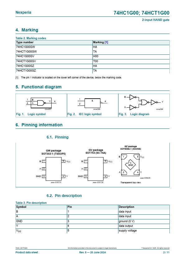
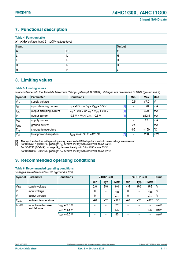
The 74HC1G00; 74HCT1G00 is a single 2-input NAND gate.
Inputs include clamp diodes .
This enables the use of current limiting resistors to interface inputs to voltages in excess of VCC.
| Part number | 74HCT1G00GZ |
|---|---|
| Manufacturer | Nexperia |
| File Size | 226.53 KB |
| Description | 2-input NAND gate |
| Datasheet |
74HCT1G00GZ Datasheet
|
|
|
|
| Part Number | Description | Manufacturer |
|---|---|---|
| 74HCT1G00 | 2-input NAND gate | Philips |
| 74HCT1G02 | 2-input NOR gate | Philips |
| 74HCT1G04 | Inverter | NXP |
| 74HCT1G08 | 2-input AND gate | NXP |
| 74HCT1G08 | 2-input AND gate | Philips |
| Part Number | Description |
|---|---|
| 74HCT1G00GV | 2-input NAND gate |
| 74HCT1G00GW | 2-input NAND gate |
| 74HCT1G00 | 2-input NAND gate |
| 74HCT1G00-Q100 | 2-input NAND gate |
| 74HCT1G02 | 2-input NOR gate |