Datasheet Details
| Part number | 74AVC16374-Q100 |
|---|---|
| Manufacturer | Nexperia |
| File Size | 766.95 KB |
| Description | 16-bit edge triggered D-type flip-flop |
| Datasheet |
 74AVC16374-Q100 Datasheet 74AVC16374-Q100 Datasheet
|
|
|
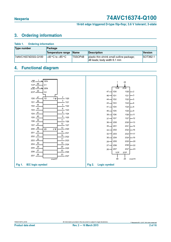
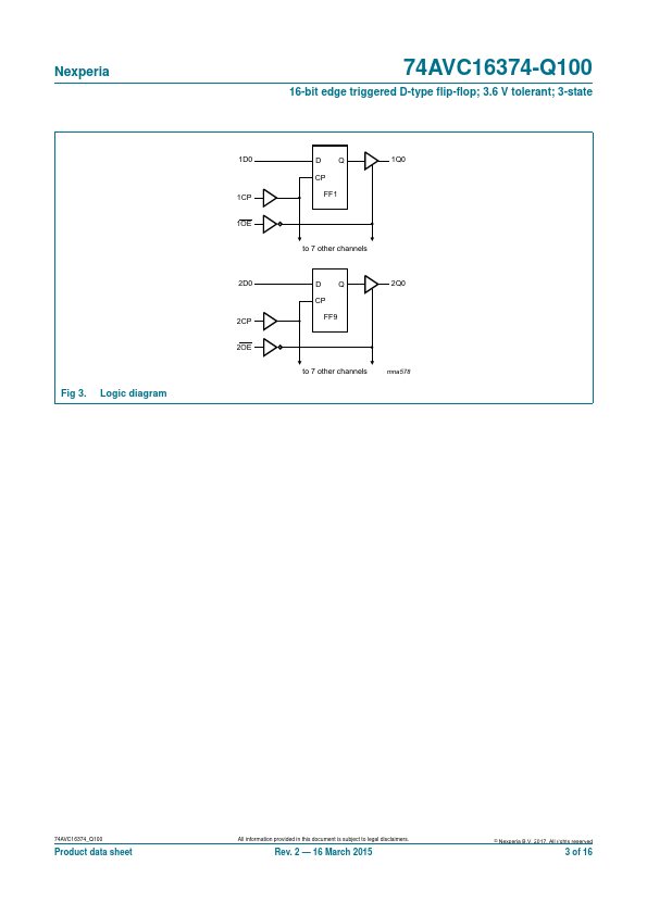
The 74AVC16374-Q100 is a 16-bit edge triggered flip-flop featuring separate D-type inputs for each flip-flop and 3-state outputs for bus-oriented applications.
The 74AVC16374-Q100 consist of 2 sections of 8 edge-triggered flip-flops.
| Part number | 74AVC16374-Q100 |
|---|---|
| Manufacturer | Nexperia |
| File Size | 766.95 KB |
| Description | 16-bit edge triggered D-type flip-flop |
| Datasheet |
74AVC16374-Q100 Datasheet
|
|
|
|
Note: Below is a high-fidelity text extraction (approx. 800 characters) for 74AVC16374-Q100. For precise diagrams, and layout, please refer to the original PDF.
74AVC16374-Q100 16-bit edge triggered D-type flip-flop; 3.6 V tolerant; 3-state Rev. 2 — 16 March 2015 Product data sheet 1. General description The 74AVC16374-Q100 is a ...
| Part Number | Description |
|---|---|
| 74AVC16374 | 16-bit edge triggered D-type flip-flop |
| 74AVC16373 | 16-bit D-type transparent latch |
| 74AVC16334A | 16-bit registered driver |
| 74AVC16244 | 16-bit buffer/line driver |
| 74AVC16245 | 16-bit transceiver |
| 74AVC16245-Q100 | 16-bit transceiver |
| 74AVC16834A | 18-bit registered driver |
| 74AVC16835A | 18-bit registered driver |
| 74AVC16836A | 20-bit registered driver |
| 74AVC16T245 | 16-bit dual supply translating transceiver |