Datasheet Details
| Part number | TPS22970 |
|---|---|
| Manufacturer | Texas Instruments |
| File Size | 1.10 MB |
| Description | On-Resistance Load Switch |
| Datasheet |
 TPS22970 Datasheet TPS22970 Datasheet
|
|
|
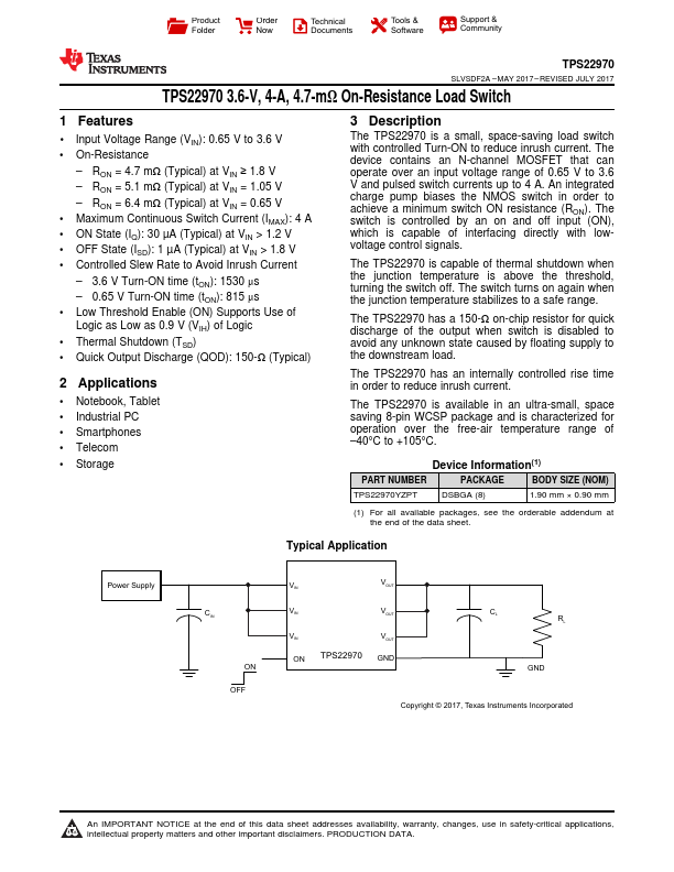
The TPS22970 is a small, space-saving load switch with controlled Turn-ON to reduce inrush current.
The device contains an N-channel MOSFET that can operate over an input voltage range of 0.65 V to 3.6 V and pulsed switch currents up to 4 A.
| Part number | TPS22970 |
|---|---|
| Manufacturer | Texas Instruments |
| File Size | 1.10 MB |
| Description | On-Resistance Load Switch |
| Datasheet |
TPS22970 Datasheet
|
|
|
|
| Part Number | Description | Manufacturer |
|---|---|---|
| TPS20 | high reliable pressure transmitter | Konics |
| TPS232 | Thermopile Sensor | PerkinElmer Optoelectronics |
| TPS2398 | -48V Hot Swap Controller | ON Semiconductor |
| TPS2399 | -48V Hot Swap Controller | ON Semiconductor |
| TPS23B | Thermopile Sensor | PerkinElmer Optoelectronics |
| Part Number | Description |
|---|---|
| TPS22971 | On-Resistance Load Switch |
| TPS22975 | On-Resistance Load Switch |
| TPS22976 | On-Resistance Dual-Channel Load Switch |
| TPS22901 | ON-Resistance Load Switch |
| TPS22902 | ON-Resistance Load Switch |
The following content is an automatically extracted verbatim text from the original manufacturer datasheet and is provided for reference purposes only.