TPA2032D1
FEATURES
- Maximize Battery Life and Minimize Heat
- 0.5-µA Shutdown Current
- 3.0-m A Quiescent Current
- High Efficiency Class-D
- 88% at 400m W at 8Ω
- 80% at 100m W at 8Ω
- Three Fixed Gain Versions
- TPA2032D1 has a gain of 2 V/V (6d B)
- TPA2033D1 has a gain of 3 V/V (9.5d B)
- TPA2034D1 has a gain of 4 V/V (12d B)
- Only One External ponent Required
- Internal Matched Input Gain and Feedback Resistors for Excellent PSRR and CMRR
- Optimized PWM Output Stage Eliminates LC Output Filter
- PSRR (- 75 d B) and Wide Supply Voltage (2.5 V to 5.5 V) Eliminates Need for a Dedicated Voltage Regulator
- Fully Differential Design Reduces RF Rectification and Eliminates Bypass Capacitor
- CMRR (- 69 d B)Eliminates Two Input Coupling Capacitors
- Thermal and Short-Circuit Protection
- Pinout Very Similar to TPA2010D1
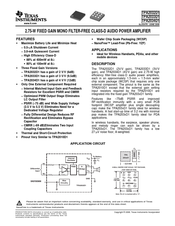
- Wafer Chip Scale Packaging (WCSP)
- Nano Free™ Lead-Free (Pb-Free: YZF)
APPLICATIONS
- Ideal for Wireless Handsets, PDAs, and other mobile devices
DESCRIPTION
The TPA2032D1 (2V/V...