Click to expand full text
SN54HC367, SN74HC367
SCLS309E – JANUARY 1996 – REVISED MARCH 2022
SNx4HC367 Hex Buffers and Line Drivers with 3-State Outputs
1 Features
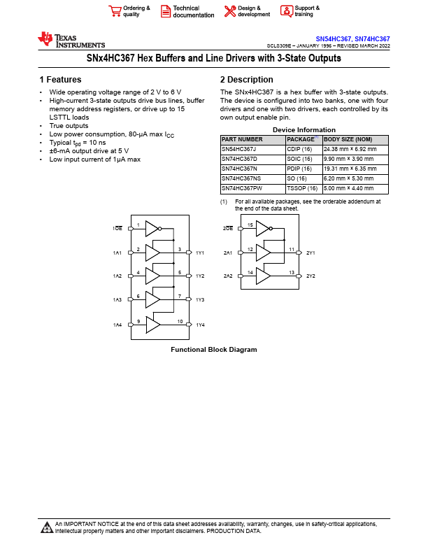
• Wide operating voltage range of 2 V to 6 V • High-current 3-state outputs drive bus lines, buffer
memory address registers, or drive up to 15 LSTTL loads • True outputs • Low power consumption, 80-μA max ICC • Typical tpd = 10 ns • ±6-mA output drive at 5 V • Low input current of 1µA max
1 1OE
2 Description
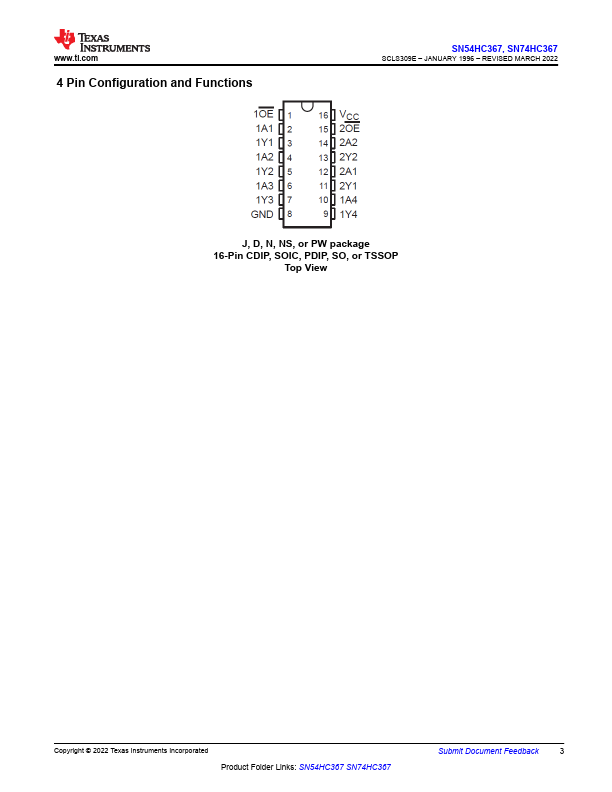
The SNx4HC367 is a hex buffer with 3-state outputs. The device is configured into two banks, one with four drivers and one with two drivers, each controlled by its own output enable pin.
PART NUMBER SN54HC367J SN74HC367D SN74HC367N SN74HC367NS SN74HC367PW
Device Information
PACKAGE(1) BODY SIZE (NOM)
CDIP (16) 24.38 mm × 6.92 mm
SOIC (16) 9.
 SN74HC367 Datasheet