Datasheet4U Logo Datasheet4U.com

SN74CBT3125D - QUADRUPLE FET BUS SWITCH

Download the SN74CBT3125D datasheet PDF. This datasheet also covers the SN74CBT3125 variant, as both devices belong to the same quadruple fet bus switch family and are provided as variant models within a single manufacturer datasheet.

Description

ordering information The SN74CBT3125 quadruple FET bus switch

Features

  • independent line switches. Each switch is disabled when the associated output-enable (OE) input is high. To ensure the high-impedance state during power up or power down, OE should be tied to VCC through a pullup resistor; the minimum value of the resistor is determined by the current-sinking capability of the driver.

📥 Download Datasheet

Note: The manufacturer provides a single datasheet file (SN74CBT3125-etcTI.pdf) that lists specifications for multiple related part numbers.

Full PDF Text Transcription

Click to expand full text
SN74CBT3125 QUADRUPLE FET BUS SWITCH 
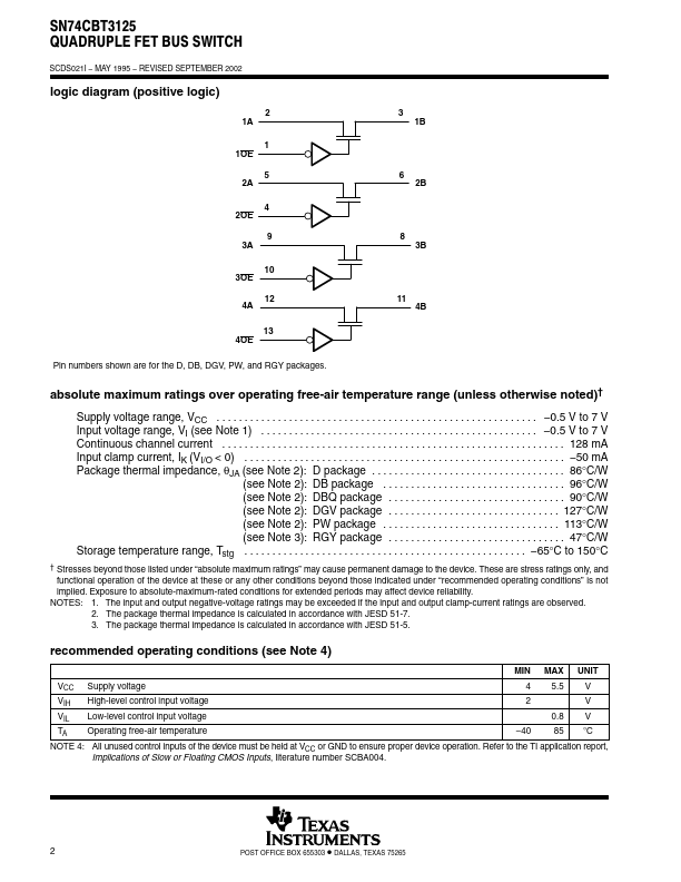
D Standard ’125-Type Pinout (D, DB, DGV, and PW Packages) SCDS021I − MAY 1995 − REVISED SEPTEMBER 2002 D 5-Ω Switch Connection Between Two Ports D TTL-Compatible Input Levels D, DB, DGV, OR PW PACKAGE (TOP VIEW) 1OE 1 1A 2 1B 3 2OE 4 2A 5 2B 6 GND 7 14 VCC 13 4OE 12 4A 11 4B 10 3OE 9 3A 8 3B RGY PACKAGE (TOP VIEW) 1OE VCC 1 1A 2 1B 3 2OE 4 2A 5 2B 6 7 14 13 4OE 12 4A 11 4B 10 3OE 9 3A 8 DBQ PACKAGE (TOP VIEW) NC 1 1OE 2 1A 3 1B 4 2OE 5 2A 6 2B 7 GND 8 16 VCC 15 4OE 14 4A 13 4B 12 3OE 11 3A 10 3B 9 NC NC − No internal connection GND 3B description/ordering information The SN74CBT3125 quadruple FET bus switch features independent line switches. Each switch is disabled when the associated output-enable (OE) input is high.
Published: |