Datasheet4U Logo Datasheet4U.com

SN74CB3Q3125 - Quadruple FET Bus Switch

Description

The SN74CB3Q3125 device is a high-bandwidth FET bus switch that uses a charge pump to elevate the gate voltage of the pass transistor, thus providing a low and flat ON-state resistance (ron).

Features

  • 1 High-Bandwidth Data Path (up to 500 MHz(1)).
  • 5-V Tolerant I/Os With Device Powered Up or Powered Down.
  • Low and Flat ON-State Resistance (ron) Characteristics Over Operating Range (ron = 3 Ω Typ).
  • Rail-to-Rail Switching on Data I/O Ports.
  • 0-V to 5-V Switching With 3.3-V VCC.
  • 0-V to 3.3-V Switching With 2.5-V VCC.
  • Bidirectional Data Flow With Near-Zero Propagation Delay.
  • Low Input and Output Capacitance Minimizes Loading and.

📥 Download Datasheet

Full PDF Text Transcription

Click to expand full text
Product Folder Sample & Buy Technical Documents Tools & Software Support & Community Reference Design SN74CB3Q3125 SCDS143C – OCTOBER 2003 – REVISED JUNE 2015 
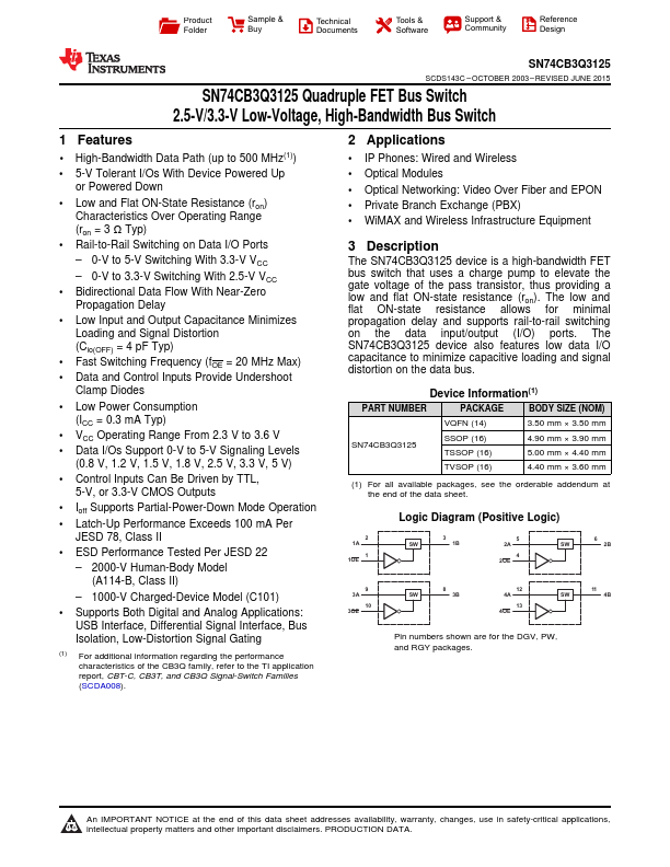
SN74CB3Q3125 Quadruple FET Bus Switch 2.5-V/3.3-V Low-Voltage, High-Bandwidth Bus Switch 1 Features •1 High-Bandwidth Data Path (up to 500 MHz(1)) • 5-V Tolerant I/Os With Device Powered Up or Powered Down • Low and Flat ON-State Resistance (ron) Characteristics Over Operating Range (ron = 3 Ω Typ) • Rail-to-Rail Switching on Data I/O Ports – 0-V to 5-V Switching With 3.3-V VCC – 0-V to 3.3-V Switching With 2.
Published: |