Click to expand full text
Product Folder
Sample & Buy
Technical Documents
Tools & Software
Support & Community
Reference Design
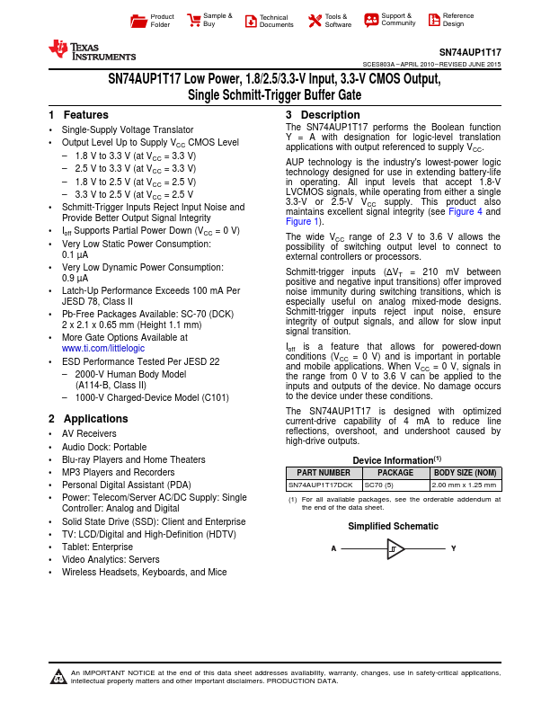
SN74AUP1T17
SCES803A – APRIL 2010 – REVISED JUNE 2015
SN74AUP1T17 Low Power, 1.8/2.5/3.3-V Input, 3.3-V CMOS Output, Single Schmitt-Trigger Buffer Gate
1 Features
•1 Single-Supply Voltage Translator • Output Level Up to Supply VCC CMOS Level
– 1.8 V to 3.3 V (at VCC = 3.3 V) – 2.5 V to 3.3 V (at VCC = 3.3 V) – 1.8 V to 2.5 V (at VCC = 2.5 V) – 3.3 V to 2.5 V (at VCC = 2.5 V • Schmitt-Trigger Inputs Reject Input Noise and Provide Better Output Signal Integrity • Ioff Supports Partial Power Down (VCC = 0 V) • Very Low Static Power Consumption: 0.1 µA • Very Low Dynamic Power Consumption: 0.
 SN74AUP1T17 Datasheet