Click to expand full text
www.ti.com
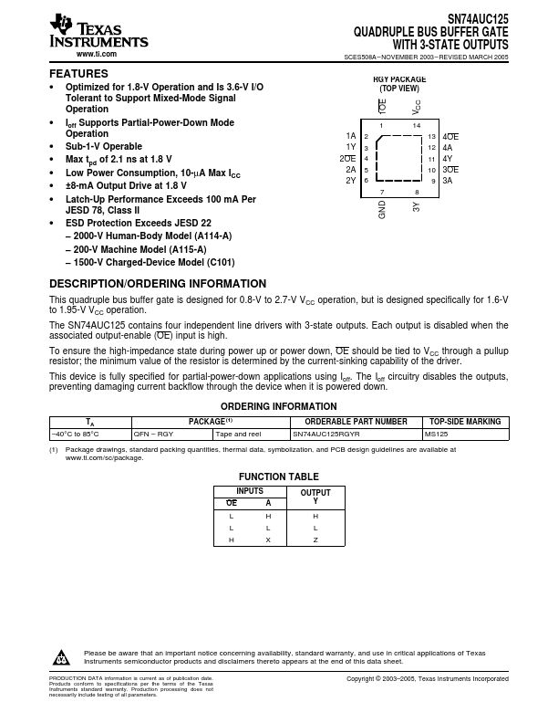
FEATURES
• Optimized for 1.8-V Operation and Is 3.6-V I/O Tolerant to Support Mixed-Mode Signal Operation
• Ioff Supports Partial-Power-Down Mode Operation
• Sub-1-V Operable • Max tpd of 2.1 ns at 1.8 V • Low Power Consumption, 10-µA Max ICC • ±8-mA Output Drive at 1.8 V • Latch-Up Performance Exceeds 100 mA Per
JESD 78, Class II • ESD Protection Exceeds JESD 22
– 2000-V Human-Body Model (A114-A) – 200-V Machine Model (A115-A) – 1500-V Charged-Device Model (C101)
GND 3Y
SN74AUC125 QUADRUPLE BUS BUFFER GATE
WITH 3-STATE OUTPUTS
SCES508A – NOVEMBER 2003 – REVISED MARCH 2005
RGY PACKAGE (TOP VIEW)
1OE VCC
1 1A 2 1Y 3 2OE 4 2A 5 2Y 6
7
14 13 4OE 12 4A 11 4Y 10 3OE 9 3A
8
DESCRIPTION/ORDERING INFORMATION
This quadruple bus buffer gate is designed for 0.8-V to 2.
 SN74AUC125 Datasheet