Click to expand full text
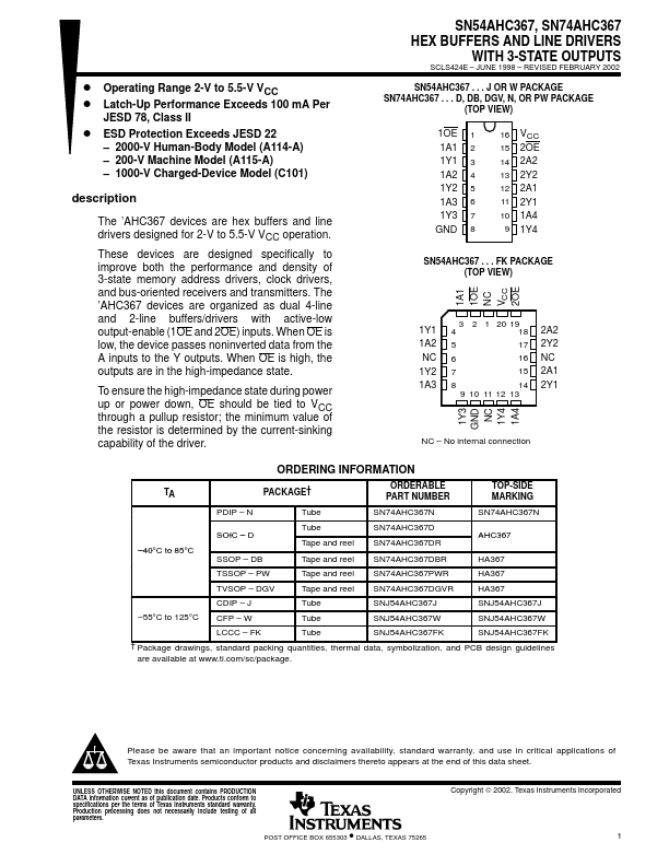
D Operating Range 2-V to 5.5-V VCC D Latch-Up Performance Exceeds 100 mA Per
JESD 78, Class II
D ESD Protection Exceeds JESD 22
– 2000-V Human-Body Model (A114-A) – 200-V Machine Model (A115-A) – 1000-V Charged-Device Model (C101)
description
The ’AHC367 devices are hex buffers and line drivers designed for 2-V to 5.5-V VCC operation.
These devices are designed specifically to improve both the performance and density of 3-state memory address drivers, clock drivers, and bus-oriented receivers and transmitters. The ’AHC367 devices are organized as dual 4-line and 2-line buffers/drivers with active-low output-enable (1OE and 2OE) inputs. When OE is low, the device passes noninverted data from the A inputs to the Y outputs. When OE is high, the outputs are in the high-impedance state.
 SN74AHC367 Datasheet