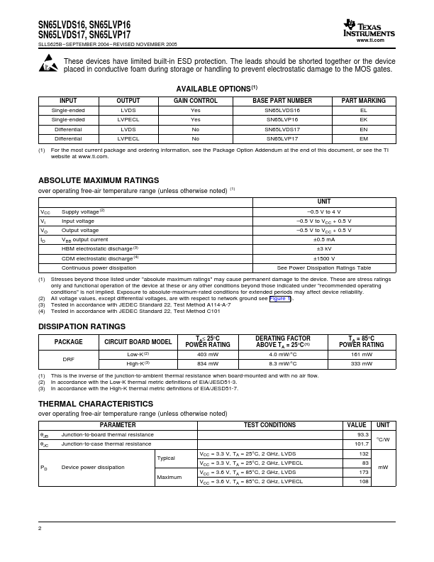
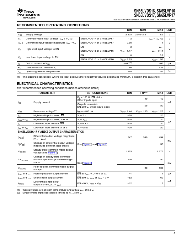
Datasheet Details
| Part number | SN65LVP17 |
|---|---|
| Manufacturer | Texas Instruments |
| File Size | 883.38 KB |
| Description | 2.5-V/3.3-V OSCILLATOR GAIN STAGE/BUFFERS |
| Datasheet |
 SN65LVP17 Datasheet SN65LVP17 Datasheet
|
|
|
Download the SN65LVP17 datasheet PDF. This datasheet also covers the SN65LVDS16 variant, as both devices belong to the same 2.5-v/3.3-v oscillator gain stage/buffers family and are provided as variant models within a single manufacturer datasheet.
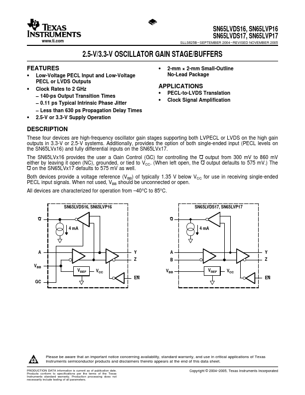
These four devices are high-frequency oscillator gain stages supporting both LVPECL or LVDS on the high gain outputs in 3.3-V or 2.5-V systems.
Additionally, provides the option of both single-ended input (PECL levels on the SN65LVx16) and fully differential inputs on the SN65LVx17.
| Part number | SN65LVP17 |
|---|---|
| Manufacturer | Texas Instruments |
| File Size | 883.38 KB |
| Description | 2.5-V/3.3-V OSCILLATOR GAIN STAGE/BUFFERS |
| Datasheet |
SN65LVP17 Datasheet
|
|
|
|
| Part Number | Description | Manufacturer |
|---|---|---|
| SN65004 | One Channel Direct Drive Speech Controller | SONiX Technology Company |
| SN65007 | One Channel Direct Drive Speech Controller | SONiX Technology Company |
| SN65010 | One Channel Direct Drive Speech Controller | SONiX Technology Company |
| SN65012 | One Channel Direct Drive Speech Controller | SONiX Technology Company |
| SN65016 | One Channel Direct Drive Speech Controller | SONiX Technology Company |
| Part Number | Description |
|---|---|
| SN65LVP16 | 2.5-V/3.3-V OSCILLATOR GAIN STAGE/BUFFERS |
| SN65LVP18 | 2.5-V/3.3-V OSCILLATOR GAIN STAGE/BUFFERS |
| SN65LVP19 | 2.5-V/3.3-V OSCILLATOR GAIN STAGE/BUFFERS |
| SN65LVP20 | LVPECL AND LVDS REPEATER/TRANSLATOR |
| SN65LVPE501 | Dual Channel x1 PCIe Redriver/Equalizer |