Datasheet4U Logo Datasheet4U.com

SN65LVDS822 - LVDS Receiver

Description

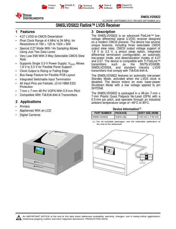
The SN65LVDS822 is an advanced FlatLink™ lowvoltage differential signal (LVDS) receiver designed on a modern CMOS process.

Features

  • 1 4:27 LVDS-to-CMOS Deserializer.
  • Pixel Clock Range of 4 MHz to 54 MHz, for Resolutions of 160 × 120 to 1024 × 600.
  • Special 2:27 Mode With 14x Sampling Allows Using Just Two Data Lanes.
  • Very Low EMI With 3-Way Selectable CMOS Slew Rate.
  • Supports Single 3.3-V Power Supply; VDDIO Allows 1.8 V to 3.3 V for Flexible Panel Support.
  • Clock Output is Rising or Falling Edge.
  • Bus-Swap Feature for Flexible PCB Layout.
  • Integrated Switch.

📥 Download Datasheet

Full PDF Text Transcription (Reference)

The following content is an automatically extracted verbatim text from the original manufacturer datasheet and is provided for reference purposes only.

View original datasheet text
Product Folder Sample & Buy Technical Documents Tools & Software Support & Community SN65LVDS822 SLLSEE8B – SEPTEMBER 2013 – REVISED SEPTEMBER 2014 SN65LVDS822 Flatlink™ LVDS Receiver 1 Features •1 4:27 LVDS-to-CMOS Deserializer • Pixel Clock Range of 4 MHz to 54 MHz, for Resolutions of 160 × 120 to 1024 × 600 • Special 2:27 Mode With 14x Sampling Allows Using Just Two Data Lanes • Very Low EMI With 3-Way Selectable CMOS Slew Rate • Supports Single 3.3-V Power Supply; VDDIO Allows 1.8 V to 3.3 V for Flexible Panel Support • Clock Output is Rising or Falling Edge • Bus-Swap Feature for Flexible PCB Layout • Integrated Switchable Input Termination • All Input Pins are Failsafe; ±3 kV HBM ESD Protection • 7-mm x 7-mm 48-Pin VQFN With 0.
Published: |