Datasheet4U Logo Datasheet4U.com

SN65LVDS109 - DUAL 4-PORT AND DUAL 8-PORT LVDS REPEATERS

Datasheet Summary

Description

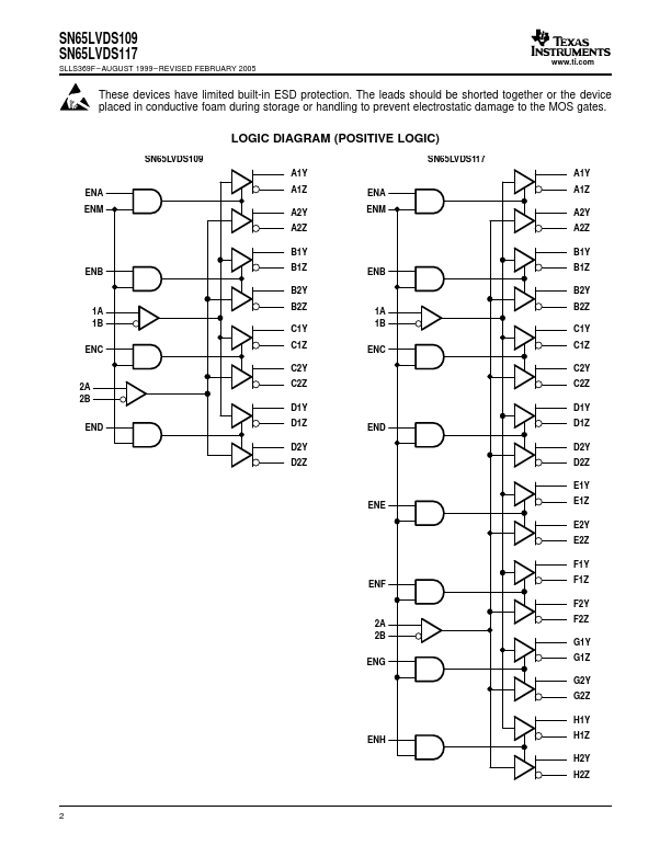
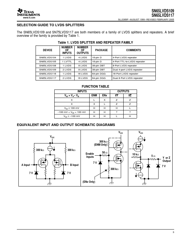
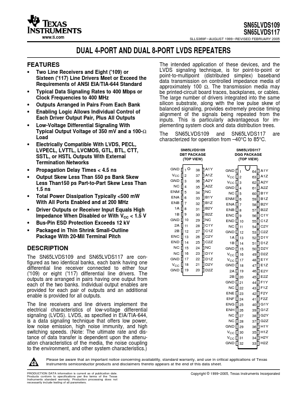
The SN65LVDS109 and SN65LVDS117 are configured as two identical banks, each bank having one differential line receiver connected to either four ('109) or eight ('117) differential line drivers.

The outputs are arranged in pairs having one output from each of the two banks.

Features

  • Two Line Receivers and Eight ('109) or Sixteen ('117) Line Drivers Meet or Exceed the Requirements of ANSI EIA/TIA-644 Standard.
  • Typical Data Signaling Rates to 400 Mbps or Clock Frequencies to 400 MHz.
  • Outputs Arranged in Pairs From Each Bank.
  • Enabling Logic Allows Individual Control of Each Driver Output Pair, Plus All Outputs.
  • Low-Voltage Differential Signaling With Typical Output Voltage of 350 mV and a 100-Ω Load.
  • Electrically Compatibl.

📥 Download Datasheet

Datasheet preview – SN65LVDS109

Datasheet Details

Part number SN65LVDS109
Manufacturer Texas Instruments
File Size 448.02 KB
Description DUAL 4-PORT AND DUAL 8-PORT LVDS REPEATERS
Datasheet download datasheet SN65LVDS109 Datasheet
Additional preview pages of the SN65LVDS109 datasheet.
Other Datasheets by Texas Instruments

Full PDF Text Transcription

Click to expand full text
www.ti.com SN65LVDS109 SN65LVDS117 SLLS369F – AUGUST 1999 – REVISED FEBRUARY 2005 DUAL 4-PORT AND DUAL 8-PORT LVDS REPEATERS FEATURES • Two Line Receivers and Eight ('109) or Sixteen ('117) Line Drivers Meet or Exceed the Requirements of ANSI EIA/TIA-644 Standard • Typical Data Signaling Rates to 400 Mbps or Clock Frequencies to 400 MHz • Outputs Arranged in Pairs From Each Bank • Enabling Logic Allows Individual Control of Each Driver Output Pair, Plus All Outputs • Low-Voltage Differential Signaling With Typical Output Voltage of 350 mV and a 100-Ω Load • Electrically Compatible With LVDS, PECL, LVPECL, LVTTL, LVCMOS, GTL, BTL, CTT, SSTL, or HSTL Outputs With External Termination Networks • Propagation Delay Times < 4.
Published: |