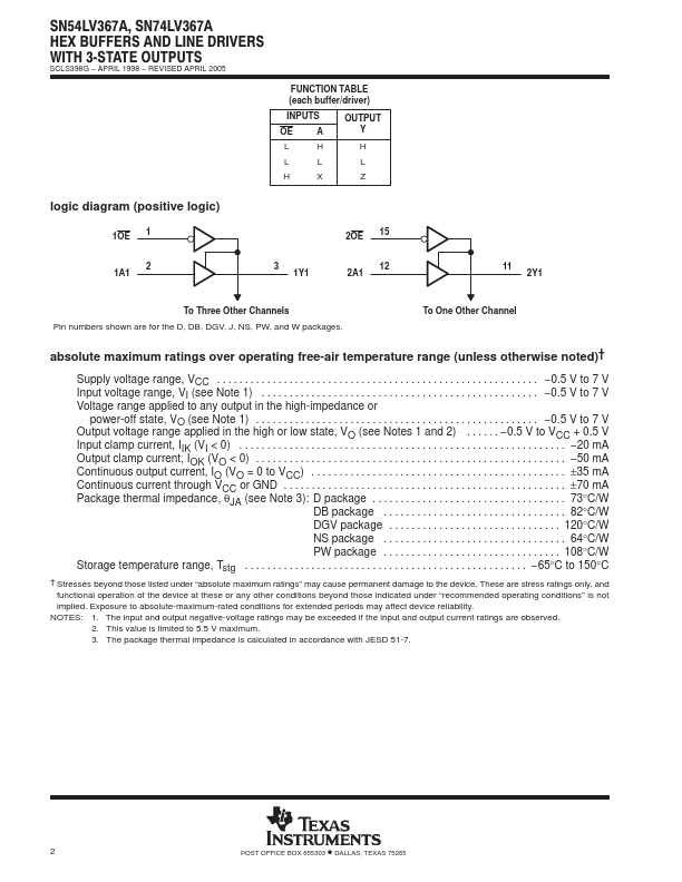
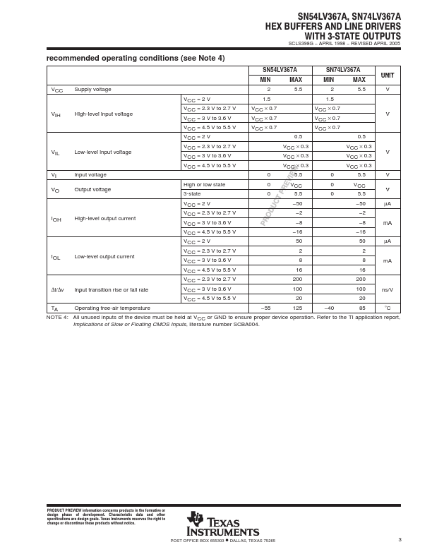
Click to expand full text
D 2-V to 5.5-V VCC Operation D Max tpd of 7 ns at 5 V D Typical VOLP (Output Ground Bounce)
<0.8 V at VCC = 3.3 V, TA = 25°C
D Typical VOHV (Output VOH Undershoot)
>2.3 V at VCC = 3.3 V, TA = 25°C
D Support Mixed-Mode Voltage Operation on
All Ports
D Latch-Up Performance Exceeds 100 mA Per
JESD 78, Class II
D ESD Protection Exceeds JESD 22
− 2000-V Human-Body Model (A114-A)
− 200-V Machine Model (A115-A)
− 1000-V Charged-Device Model (C101)
SN54LV367A, SN74LV367A HEX BUFFERS AND LINE DRIVERS
WITH 3ĆSTATE OUTPUTS
SCLS398G − APRIL 1998 − REVISED APRIL 2005
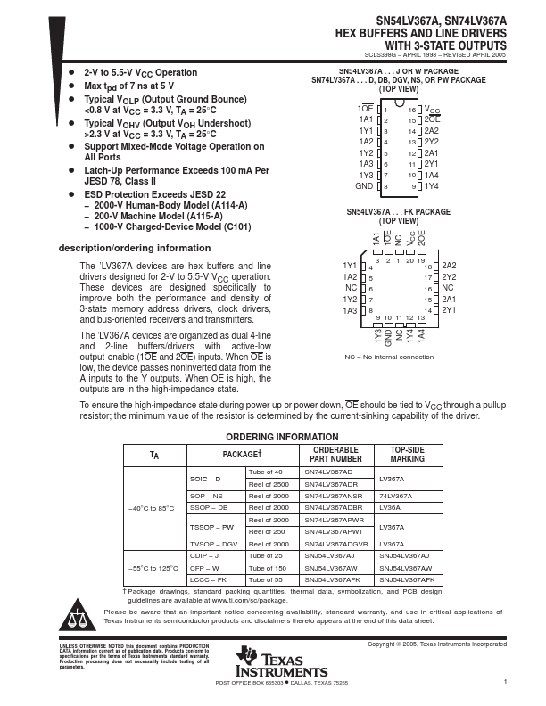
SN54LV367A . . . J OR W PACKAGE SN74LV367A . . . D, DB, DGV, NS, OR PW PACKAGE
(TOP VIEW)
1OE 1 1A1 2 1Y1 3 1A2 4 1Y2 5 1A3 6 1Y3 7 GND 8
16 VCC 15 2OE 14 2A2 13 2Y2 12 2A1 11 2Y1 10 1A4 9 1Y4
SN54LV367A . . .
 SN54LV367A Datasheet