Datasheet Details
| Part number | DS90CR286AT-Q1 |
|---|---|
| Manufacturer | Texas Instruments |
| File Size | 2.08 MB |
| Description | 3.3 V Rising Edge Data Strobe LVDS Receiver |
| Datasheet |
 DS90CR286AT-Q1 Datasheet DS90CR286AT-Q1 Datasheet
|
|
|
| Part number | DS90CR286AT-Q1 |
|---|---|
| Manufacturer | Texas Instruments |
| File Size | 2.08 MB |
| Description | 3.3 V Rising Edge Data Strobe LVDS Receiver |
| Datasheet |
DS90CR286AT-Q1 Datasheet
|
|
|
|
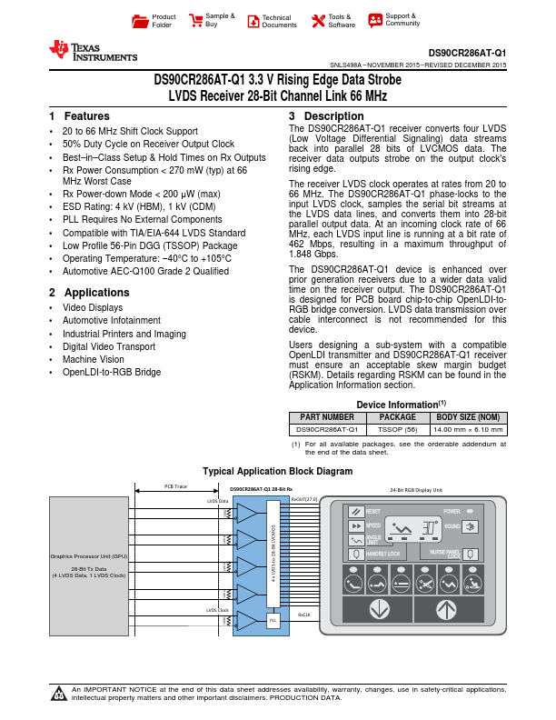
The DS90CR286AT-Q1 receiver converts four LVDS (Low Voltage Differential Signaling) data streams back into parallel 28 bits of LVCMOS data.
The receiver data outputs strobe on the output clock's rising edge.
The receiver LVDS clock operates at rates from 20 to 66 MHz.
Product Folder Sample & Buy Technical Documents Tools & Software Support & Community DS90CR286AT-Q1 SNLS498A – NOVEMBER 2015 – REVISED DECEMBER 2015 DS90CR286AT-Q1 3.
| Part Number | Description |
|---|---|
| DS90CR286A | 3.3-V Rising Edge Data Strobe LVDS Receiver |
| DS90CR286 | +3.3V Rising Edge Data Strobe LVDS |
| DS90CR285 | +3.3V Rising Edge Data Strobe LVDS |
| DS90CR287 | +3.3V Rising Edge Data Strobe LVDS |
| DS90CR288A | +3.3V Rising Edge Data Strobe LVDS |
| DS90CR215 | +3.3V Rising Edge Data Strobe LVDS |
| DS90CR216 | +3.3V Rising Edge Data Strobe LVDS |
| DS90CR216A | 3.3-V Rising Edge Data Strobe LVDS Receiver |
| DS90CR216A-Q1 | 3.3-V Rising Edge Data Strobe LVDS Receiver |
| DS90CR217 | +3.3V Rising Edge Data Strobe LVDS |