Click to expand full text
Product Folder
Sample & Buy
Technical Documents
Tools & Software
Support & Community
CSD17581Q5A
SLPS630 – SEPTEMBER 2016
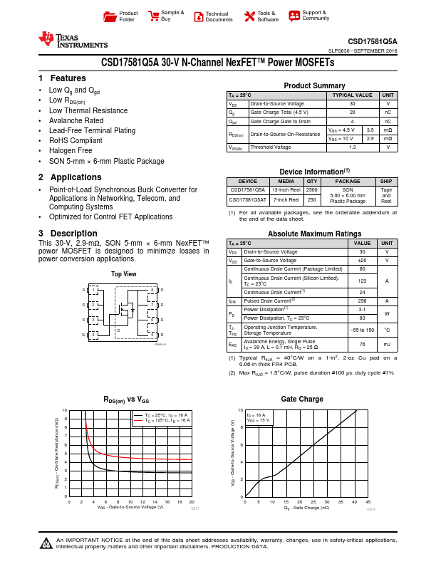
CSD17581Q5A 30-V N-Channel NexFET™ Power MOSFETs
1 Features
•1 Low Qg and Qgd • Low RDS(on) • Low Thermal Resistance • Avalanche Rated • Lead-Free Terminal Plating • RoHS Compliant • Halogen Free • SON 5-mm × 6-mm Plastic Package
2 Applications
• Point-of-Load Synchronous Buck Converter for Applications in Networking, Telecom, and Computing Systems
• Optimized for Control FET Applications
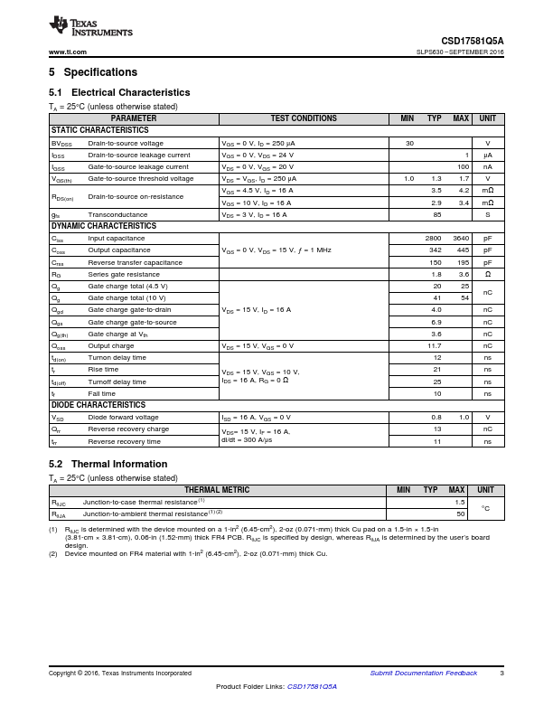
Product Summary
TA = 25°C VDS Drain-to-Source Voltage Qg Gate Charge Total (4.5 V) Qgd Gate Charge Gate to Drain
RDS(on) Drain-to-Source On-Resistance
VGS(th) Threshold Voltage
TYPICAL VALUE
30
20
4
VGS = 4.5 V VGS = 10 V
1.3
3.5 2.9
UNIT V nC nC mΩ mΩ V
.
 CSD17581Q5A Datasheet