Datasheet4U Logo Datasheet4U.com

CDCUN1208LP - 400-MHz Low Power 2:8 Fan-Out Buffer

Datasheet Summary

Description

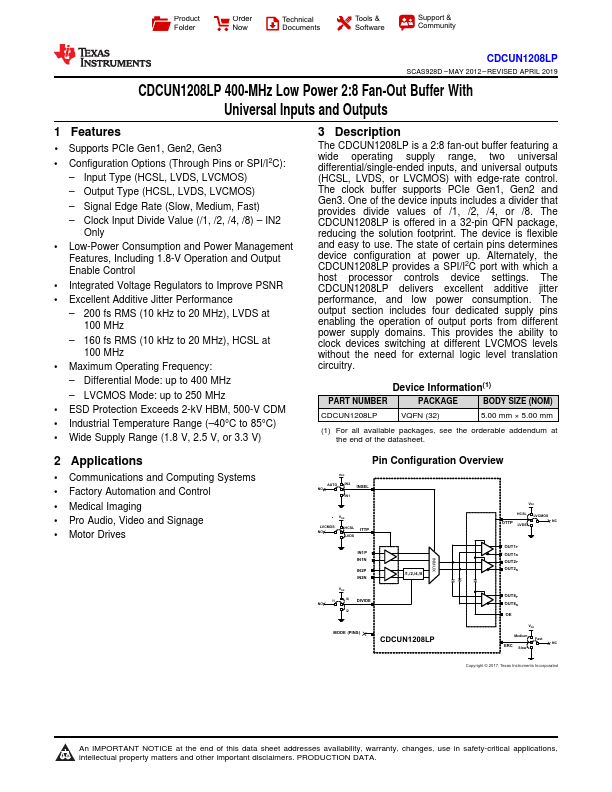
The CDCUN1208LP is a 2:8 fan-out buffer featuring a wide operating supply range, two universal differential/single-ended inputs, and universal outputs (HCSL, LVDS, or LVCMOS) with edge-rate control.

The clock buffer supports PCIe Gen1, Gen2 and Gen3.

Features

  • 1 Supports PCIe Gen1, Gen2, Gen3.
  • Configuration Options (Through Pins or SPI/I2C):.
  • Input Type (HCSL, LVDS, LVCMOS).
  • Output Type (HCSL, LVDS, LVCMOS).
  • Signal Edge Rate (Slow, Medium, Fast).
  • Clock Input Divide Value (/1, /2, /4, /8).
  • IN2 Only.
  • Low-Power Consumption and Power Management Features, Including 1.8-V Operation and Output Enable Control.
  • Integrated Voltage Regulators to Improve PSNR.
  • Excellent Addi.

📥 Download Datasheet

Datasheet preview – CDCUN1208LP

Datasheet Details

Part number CDCUN1208LP
Manufacturer Texas Instruments
File Size 2.21 MB
Description 400-MHz Low Power 2:8 Fan-Out Buffer
Datasheet download datasheet CDCUN1208LP Datasheet
Additional preview pages of the CDCUN1208LP datasheet.
Other Datasheets by Texas Instruments

Full PDF Text Transcription

Click to expand full text
Product Folder Order Now Technical Documents Tools & Software Support & Community CDCUN1208LP SCAS928D – MAY 2012 – REVISED APRIL 2019 CDCUN1208LP 400-MHz Low Power 2:8 Fan-Out Buffer With Universal Inputs and Outputs 1 Features •1 Supports PCIe Gen1, Gen2, Gen3 • Configuration Options (Through Pins or SPI/I2C): – Input Type (HCSL, LVDS, LVCMOS) – Output Type (HCSL, LVDS, LVCMOS) – Signal Edge Rate (Slow, Medium, Fast) – Clock Input Divide Value (/1, /2, /4, /8) – IN2 Only • Low-Power Consumption and Power Management Features, Including 1.
Published: |