Click to expand full text
CDCLVC1310
www.ti.com
SCAS917E – JULY 2011 – REVISED JANUARY 2014
Ten-Output Low-Jitter Low-Power Clock Buffer and Level Translator
Check for Samples: CDCLVC1310
FEATURES
1
• High-Performance Crystal Buffer With Ultralow Noise Floor of –169 dBc/Hz
• Additive Phase Noise/Jitter Performance Is 25 fsRMS (Typ.)
• Level Translation With 3.3-V or 2.5-V Core and 3.3-V, 2.5-V, 1.8-V, or 1.5-V Output Supply
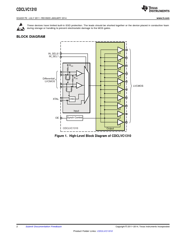
• Device inputs consist of primary, secondary, and crystal inputs, and manually selectable (through pins) using the input MUX. The primary and secondary inputs can accept LVPECL, LVDS, HCSL, SSTL or LVCMOS signals and crystal input.
 CDCLVC1310 Datasheet