Datasheet4U Logo Datasheet4U.com

CDCF2510 - 3.3-V Phase-Lock Loop Clock Driver

Description

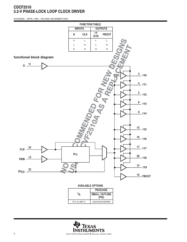
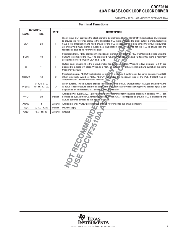
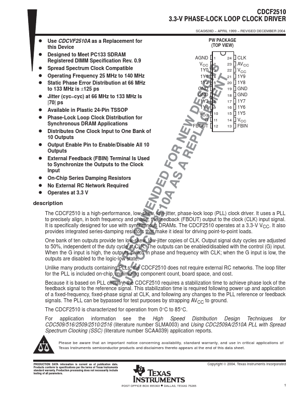
The CDCF2510 is a high-performance, low-skew, low-jitter, phase-lock loop (PLL) clock driver.

It uses a PLL to precisely align, in both frequency and phase, the feedback (FBOUT) output to the clock (CLK) input signal.

It is specifically designed for use with synchronous DRAMs.

📥 Download Datasheet

Datasheet preview – CDCF2510

Datasheet Details

Part number CDCF2510
Manufacturer Texas Instruments
File Size 474.01 KB
Description 3.3-V Phase-Lock Loop Clock Driver
Datasheet download datasheet CDCF2510 Datasheet
Additional preview pages of the CDCF2510 datasheet.
Other Datasheets by Texas Instruments

Full PDF Text Transcription

Click to expand full text
CDCF2510 3.3ĆV PHASEĆLOCK LOOP CLOCK DRIVER ą SCAS628D − APRIL 1999 − REVISED DECEMBER 2004 D Use CDCVF2510A as a Replacement for this Device D Designed to Meet PC133 SDRAM Registered DIMM Specification Rev. 0.9 D Spread Spectrum Clock Compatible D Operating Frequency 25 MHz to 140 MHz D Static Phase Error Distribution at 66 MHz to 133 MHz is ±125 ps D Jitter (cyc−cyc) at 66 MHz to 133 MHz Is |70| ps D Available in Plastic 24-Pin TSSOP D Phase-Lock Loop Clock Distribution for Synchronous DRAM Applications D Distributes One Clock Input to One Bank of 10 Outputs D Output Enable Pin to Enable/Disable All 10 Outputs D External Feedback (FBIN) Terminal Is Used to Synchronize the Outputs to the Clock Input D On-Chip Series Damping Resistors D No External RC Network Required D Operates at 3.
Published: |