Datasheet4U Logo Datasheet4U.com

CDCDB2000 - 20-Output Clock Buffer

Description

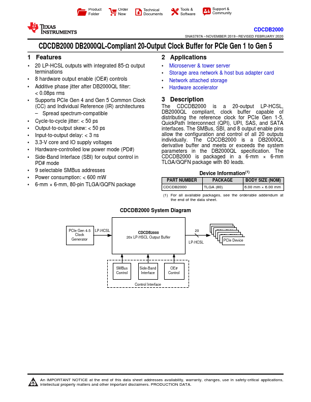
The CDCDB2000 is a 20-output LP-HCSL, DB2000QL compliant, clock buffer capable of distributing the reference clock for PCIe Gen 1-5, QuickPath Interconnect (QPI), UPI, SAS, and SATA interfaces.

Features

  • 1 20 LP-HCSL outputs with integrated 85-Ω output terminations.
  • 8 hardware output enable (OE#) controls.
  • Additive phase jitter after DB2000QL filter: < 0.08ps rms.
  • Supports PCIe Gen 4 and Gen 5 Common Clock (CC) and Individual Reference (IR) architectures.
  • Spread spectrum-compatible.
  • Cycle-to-cycle jitter: < 50 ps.
  • Output-to-output skew: < 50 ps.
  • Input-to-output delay: < 3 ns.
  • 3.3-V core and IO supply voltages.

📥 Download Datasheet

Datasheet preview – CDCDB2000

Datasheet Details

Part number CDCDB2000
Manufacturer Texas Instruments
File Size 1.24 MB
Description 20-Output Clock Buffer
Datasheet download datasheet CDCDB2000 Datasheet
Additional preview pages of the CDCDB2000 datasheet.
Other Datasheets by Texas Instruments

Full PDF Text Transcription

Click to expand full text
Product Folder Order Now Technical Documents Tools & Software Support & Community CDCDB2000 SNAS787A – NOVEMBER 2019 – REVISED FEBRUARY 2020 CDCDB2000 DB2000QL-Compliant 20-Output Clock Buffer for PCIe Gen 1 to Gen 5 1 Features •1 20 LP-HCSL outputs with integrated 85-Ω output terminations • 8 hardware output enable (OE#) controls • Additive phase jitter after DB2000QL filter: < 0.08ps rms • Supports PCIe Gen 4 and Gen 5 Common Clock (CC) and Individual Reference (IR) architectures – Spread spectrum-compatible • Cycle-to-cycle jitter: < 50 ps • Output-to-output skew: < 50 ps • Input-to-output delay: < 3 ns • 3.
Published: |