Datasheet Details
| Part number | CD74HCT365-Q1 |
|---|---|
| Manufacturer | Texas Instruments |
| File Size | 773.25 KB |
| Description | High-Speed CMOS Logic HEX Buffer/Line Driver |
| Datasheet |
 CD74HCT365-Q1 Datasheet CD74HCT365-Q1 Datasheet
|
|
|
Download the CD74HCT365-Q1 datasheet PDF. This datasheet also covers the CD74HC365-Q1 variant, as both devices belong to the same high-speed cmos logic hex buffer/line driver family and are provided as variant models within a single manufacturer datasheet.
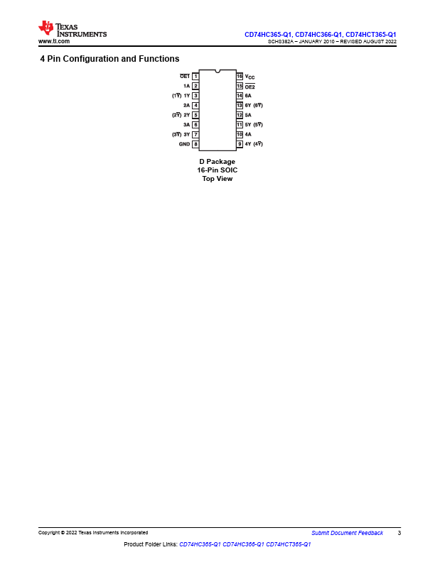
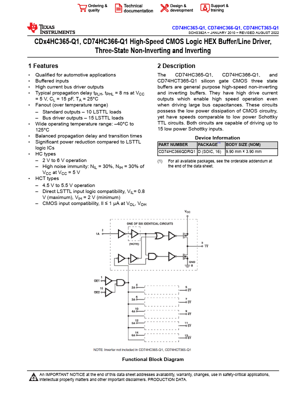
The CD74HC365-Q1, CD74HC366-Q1, and CD74HCT365-Q1 silicon gate CMOS three state buffers are general purpose high-speed non-inverting and inverting buffers.
They have high drive current outputs which enable high speed operation even when driving large bus capacitances.
| Part number | CD74HCT365-Q1 |
|---|---|
| Manufacturer | Texas Instruments |
| File Size | 773.25 KB |
| Description | High-Speed CMOS Logic HEX Buffer/Line Driver |
| Datasheet |
CD74HCT365-Q1 Datasheet
|
|
|
|
Note: Below is a high-fidelity text extraction (approx. 800 characters) for CD74HCT365-Q1. For precise diagrams, and layout, please refer to the original PDF.
CD74HC365-Q1, CD74HC366-Q1, CD74HCT365-Q1 SCHS382A – JANUARY 2010 – REVISED AUGUST 2022 CDx4HC365-Q1, CD74HC366-Q1 High-Speed CMOS Logic HEX Buffer/Line Driver, Three-Sta...
| Part Number | Description |
|---|---|
| CD74HCT365 | High Speed CMOS Logic Hex Buffer/Line Driver |
| CD74HCT365E | High Speed CMOS Logic Hex Buffer/Line Driver |
| CD74HCT365M | High Speed CMOS Logic Hex Buffer/Line Driver |
| CD74HCT367 | Three-State Non-Inverting and Inverting |
| CD74HCT367E | Three-State Non-Inverting and Inverting |
| CD74HCT367M | Three-State Non-Inverting and Inverting |
| CD74HCT367M96 | Three-State Non-Inverting and Inverting |
| CD74HCT367MT | Three-State Non-Inverting and Inverting |
| CD74HCT368 | Three-State Non-Inverting and Inverting |
| CD74HCT368E | Three-State Non-Inverting and Inverting |