CD74FCT564
Features
- Buffered Inputs
NOFOUTs RRe ECNCMEOOWSMDTMe Ec Eh SNn Io GDlo NEg SDy
- Typical Propagation Delay: 5.6ns at VCC = 5V, TA = 25o C
- Positive Edge Triggered
- CD74FCT564
- Inverting
- CD74FCT574
- Noninverting
- SCR Latchup Resistant Bi CMOS Process and Circuit Design
- Speed of Bipolar FAST™/AS/S
- 48m A Output Sink Current
- Output Voltage Swing Limited to 3.7V at VCC = 5V
- Controlled Output Edge Rates
- Input/Output Isolation to VCC
- Bi CMOS Technology with Low Quiescent Power
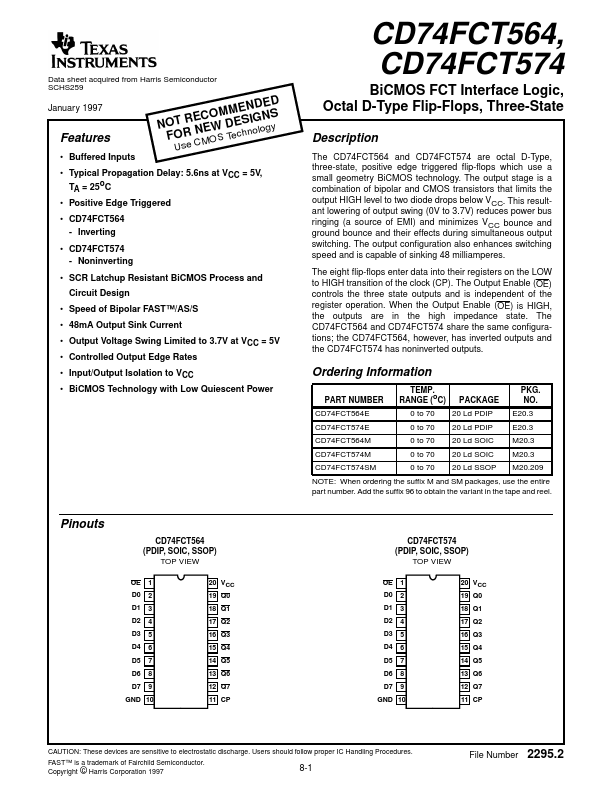
Pinouts
CD74FCT564 (PDIP, SOIC, SSOP)
TOP VIEW
OE 1 D0 2 D1 3 D2 4 D3 5 D4 6 D5 7 D6 8 D7 9 GND 10
20 VCC 19 Q0 18 Q1 17 Q2 16 Q3 15 Q4 14 Q5 13 Q6 12 Q7 11 CP
CD74FCT564, CD74FCT574
Bi CMOS FCT Interface Logic, Octal D-Type Flip-Flops, Three-State
Description
The CD74FCT564 and CD74FCT574 are octal D-Type, three-state, positive edge triggered flip-flops which use a small geometry Bi CMOS technology. The output stage is a bination of bipolar and CMOS transistors that limits the output HIGH level to...