Datasheet Details
| Part number | ADC10D040 |
|---|---|
| Manufacturer | Texas Instruments |
| File Size | 1.26 MB |
| Description | 267mW A/D Converter |
| Datasheet |
 ADC10D040 Datasheet ADC10D040 Datasheet
|
|
|
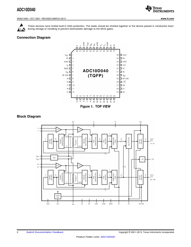
The ADC10D040 is a dual low power, high performance CMOS analog-to-digital converter that digitizes signals to 10 bits resolution at sampling rates up to 45 MSPS while consuming a typical 267 mW from a single 3.3V supply.
No missing codes is specified over the full operating temperature range.
| Part number | ADC10D040 |
|---|---|
| Manufacturer | Texas Instruments |
| File Size | 1.26 MB |
| Description | 267mW A/D Converter |
| Datasheet |
ADC10D040 Datasheet
|
|
|
|
Note: Below is a high-fidelity text extraction (approx. 800 characters) for ADC10D040. For precise diagrams, and layout, please refer to the original PDF.
ADC10D040 www.ti.com SNAS149G – OCT 2001 – REVISED MARCH 2013 ADC10D040 Dual 10-Bit, 40 MSPS, 267 mW A/D Converter Check for Samples: ADC10D040 FEATURES 1 •2 Internal Sam...
| Brand Logo | Part Number | Description | Manufacturer |
|---|---|---|---|
| ADC10D040 | A/D Converter | National Semiconductor |
| Part Number | Description |
|---|---|
| ADC10D020 | 150mW A/D Converter |
| ADC10D1000 | 10-Bit Dual ADC |
| ADC10D1000QML-SP | Low-Power 10-Bit Dual 1-GSPS or Single 2-GSPS Analog-to-Digital Converter |
| ADC10D1500 | 10-Bit Dual ADC |
| ADC10DL065 | Dual 10-Bit 65MSPS 3.3V 370mW A/D Converter |
| ADC10DV200 | Dual 10-bit 200MSPS Low-Power A/D Converter |
| ADC10040 | 10-Bit 40MSPS 3V 55.5mW A/D Converter |
| ADC10040Q | 10-Bit 40MSPS 3V 55.5mW A/D Converter |
| ADC10065 | 10-Bit 65MSPS 3V A/D Converter |
| ADC10080 | 10-Bit 80MSPS 3V 78.6mW A/D Converter |