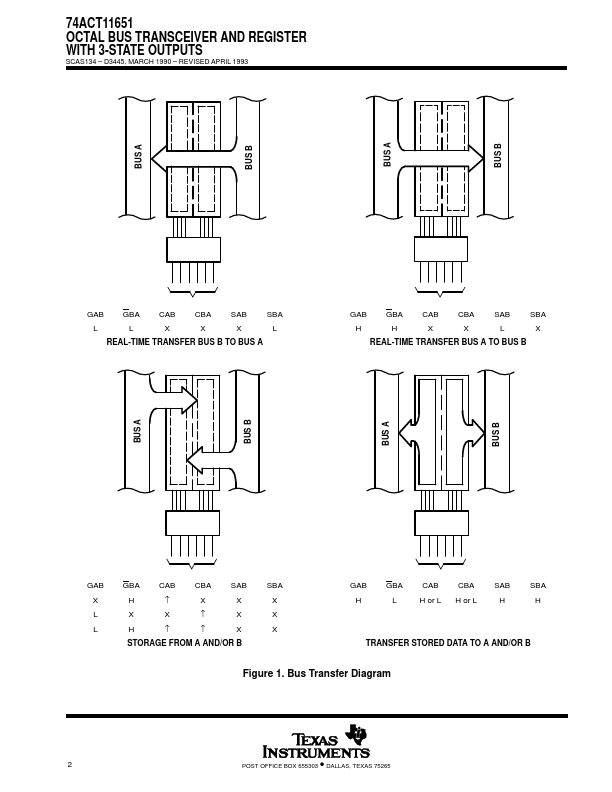
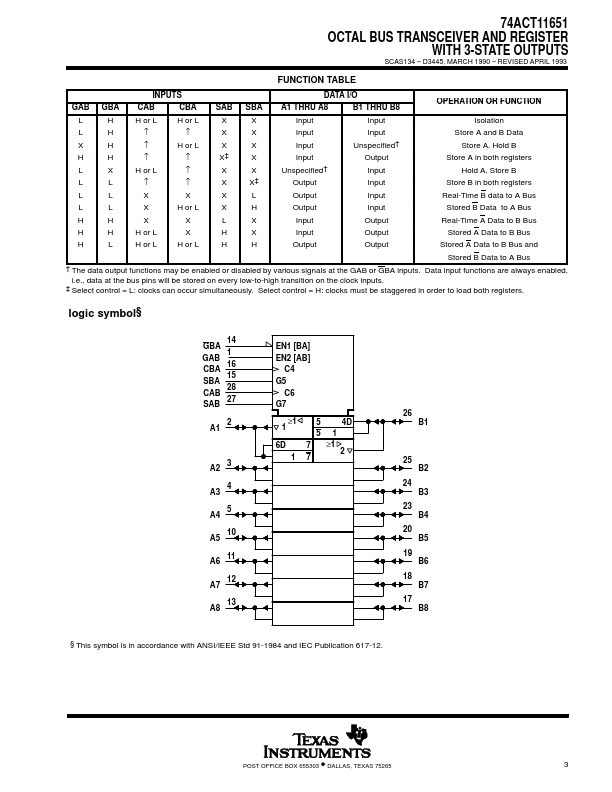
Click to expand full text
• Inputs Are TTL-Voltage Compatible • Bus Transceivers/Registers • Independent Registers and Enables for A
and B Buses
• Multiplexed Real-Time and Stored Data • Inverting Data Paths • Flow-Through Architecture to Optimize
PCB Layout
• Center-Pin VCC and GND Configurations to
Minimize High-Speed Switching Noise
t• EPIC (Enhanced-Performance Implanted CMOS) 1-mm Process
• 500-mA Typical Latch-Up Immunity
at 125°C
• Package Options Include Plastic Small
Outline Packages and Standard Plastic
300-mil DIPs
74ACT11651 OCTAL BUS TRANSCEIVER AND REGISTER
WITH 3-STATE OUTPUTS
SCAS134 – D3445, MARCH 1990 – REVISED APRIL 1993
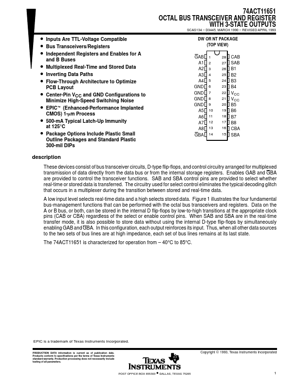
DW OR NT PACKAGE
(TOP VIEW)
GAB A1 A2 A3 A4
GND GND GND GND
A5 A6 A7 A8 GBA
1 2 3 4 5 6 7 8 9 10 11 12 13 14
28 CAB
27 SAB
26 B1
25 B2
24 B3
23 B4 22 VCC 21 VCC 20 B5 19 B6 1
 74ACT11651 Datasheet