Click to expand full text
D 3-State Outputs Drive Bus Lines Directly D Inputs Are TTL-Voltage Compatible D Flow-Through Architecture Optimizes
PCB Layout
D Center-Pin VCC and GND Configurations
Minimize High-Speed Switching Noise
D EPICt (Enhanced-Performance Implanted
CMOS) 1-mm Process
D 500-mA Typical Latch-Up Immunity at
125°C
D Package Options Include Plastic
Small-Outline (DW), Shrink Small-Outline
(DB), and Thin Shrink Small-Outline (PW)
Packages, and Standard Plastic 300-mil
DIPs (NT)
74ACT11245 OCTAL BUS TRANSCEIVER
WITH 3-STATE OUTPUTS
SCAS031C – JULY 1987 – REVISED APRIL 1996
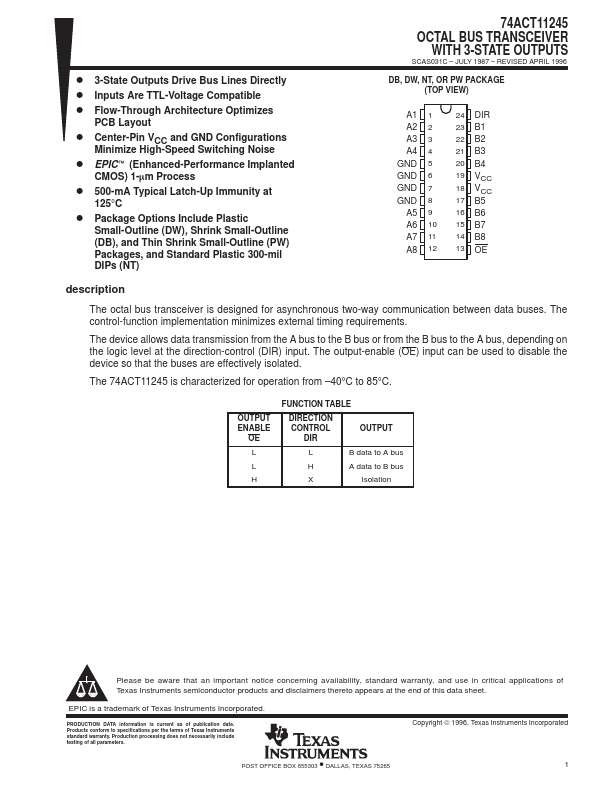
DB, DW, NT, OR PW PACKAGE (TOP VIEW)
A1 1 A2 2 A3 3 A4 4 GND 5 GND 6 GND 7 GND 8 A5 9 A6 10 A7 11 A8 12
24 DIR 23 B1 22 B2 21 B3 20 B4 19 VCC 18 VCC 17 B5 16 B6 15 B7 14 B8 13 OE
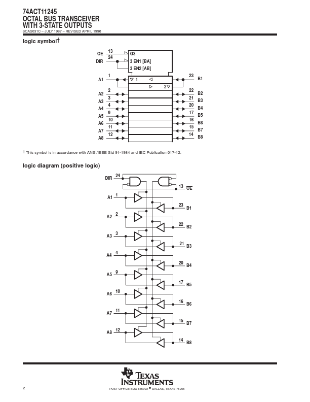
description
The octal bus transceiver is designed
 74ACT11245 Datasheet