Click to expand full text
ą
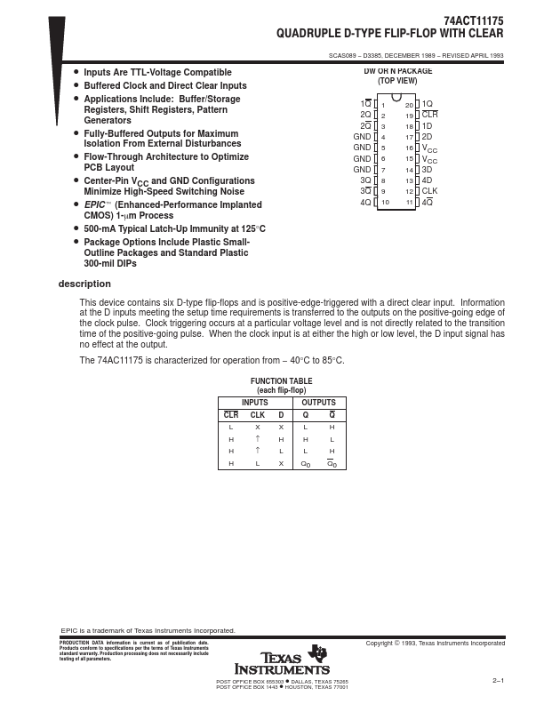
• Inputs Are TTL-Voltage Compatible • Buffered Clock and Direct Clear Inputs • Applications Include: Buffer/Storage
Registers, Shift Registers, Pattern Generators
• Fully-Buffered Outputs for Maximum
Isolation From External Disturbances
• Flow-Through Architecture to Optimize
PCB Layout
• Center-Pin VCC and GND Configurations
Minimize High-Speed Switching Noise
• EPICt (Enhanced-Performance Implanted
CMOS) 1-mm Process
• 500-mA Typical Latch-Up Immunity at 125°C • Package Options Include Plastic Small-
Outline Packages and Standard Plastic 300-mil DIPs
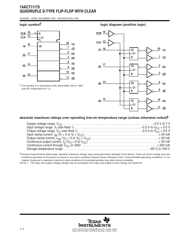
74ACT11175 QUADRUPLE DĆTYPE FLIPĆFLOP WITH CLEAR
ą
SCAS089 − D3385, DECEMBER 1989 − REVISED APRIL 1993
DW OR N PACKAGE (TOP VIEW)
1Q 2Q 2Q GND GND GND GND 3Q 3Q 4Q
1 2 3 4 5 6 7 8 9 10
20 1Q 19 CLR 18 1D 17 2D 16 VCC 15 VCC 14 3D 13 4D
 74ACT11175 Datasheet