X17256128DD8M Datasheet Text
0
R
QPRO Family of XC1700D QML Configuration PROMs
0 2
DS070 (v2.1) June 1, 2000
Product Specification
Features
- -
- Certified to MIL-PRF-38535 Appendix A QML (Qualified Manufacturer Listing.) Also available under the following Standard Microcircuit Drawings (SMD): 5962-94717 and 5962-95617. Configuration one-time programmable (OTP) read-only memory designed to store configuration bitstreams of Xilinx FPGA devices On-chip address counter, incremented by each rising edge on the clock input Simple interface to the FPGA requires only one user I/O pin Cascadable for storing longer or multiple bitstreams Programmable reset polarity (active High or active Low) for patibility with different FPGA solutions Low-power CMOS EPROM process Available in 5V version only Programming support by leading programmer manufacturers. Design support using the Xilinx Alliance and Foundation series software packages.
Description
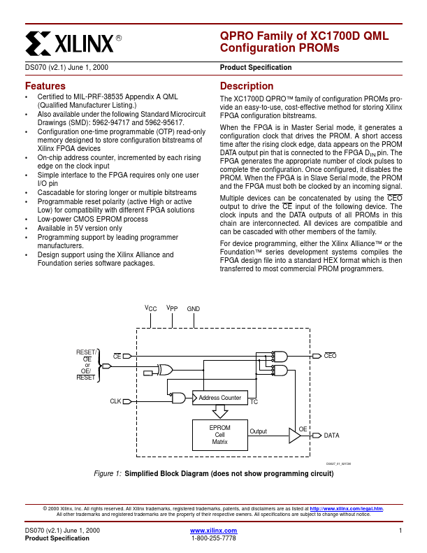
The XC1700D QPRO™ family of configuration PROMs provide an easy-to-use, cost-effective method for storing Xilinx FPGA configuration bitstreams. When the FPGA is in Master Serial mode, it generates a configuration clock that drives the PROM. A short access time after the rising clock edge, data appears on the PROM DATA output pin that is connected to the FPGA D IN pin. The FPGA generates the appropriate number of clock pulses to plete the configuration. Once configured, it disables the PROM. When the FPGA is in Slave Serial mode, the PROM and the FPGA must both be clocked by an ining signal. Multiple devices can be concatenated by using the CEO output to drive the CE input of the following device. The clock inputs and the DATA outputs of all PROMs in this chain are interconnected. All devices are patible and can be cascaded with other members of the...