WFD2N60
Features
- -
- -
- RDS(on) (Max 5.0 Ω )@VGS=10V Gate Charge (Typical 9.5n C) Improved dv/dt Capability, High Ruggedness 100% Avalanche Tested Maximum Junction Temperature Range (150°C)
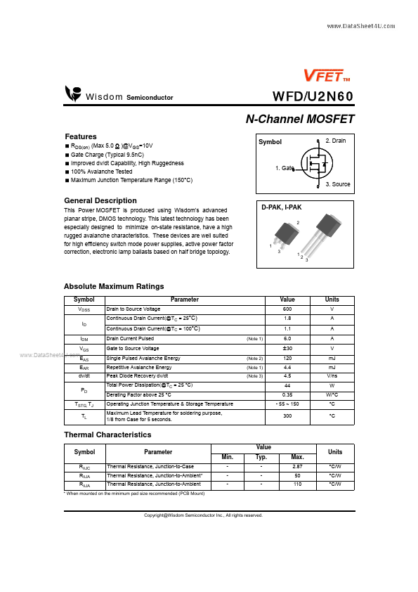
Symbol
◀
{
2. Drain
- 1. Gate {
▲
- -
{
3. Source
General Description
This Power MOSFET is produced using Wisdom’s advanced planar stripe, DMOS technology. This latest technology has been especially designed to minimize on-state resistance, have a high rugged avalanche characteristics. These devices are well suited for high efficiency switch mode power supplies, active power factor correction, electronic lamp ballasts based on half bridge topology.
D-PAK, I-PAK
1 3 1 2 3
Absolute Maximum Ratings
Symbol
VDSS ID IDM VGS Drain to Source Voltage Continuous Drain Current(@TC = 25°C) Continuous Drain Current(@TC = 100°C) Drain Current Pulsed Gate to Source Voltage Single Pulsed Avalanche Energy Repetitive Avalanche Energy Peak Diode Recovery dv/dt Total Power Dissipation(@TC = 25 °C) Derating...