The following content is an automatically extracted verbatim text
from the original manufacturer datasheet and is provided for reference purposes only.
View original datasheet text
www.DataSheet4U.com
White Electronic Designs
512KX32 SRAM / FLASH MODULE
FEATURES
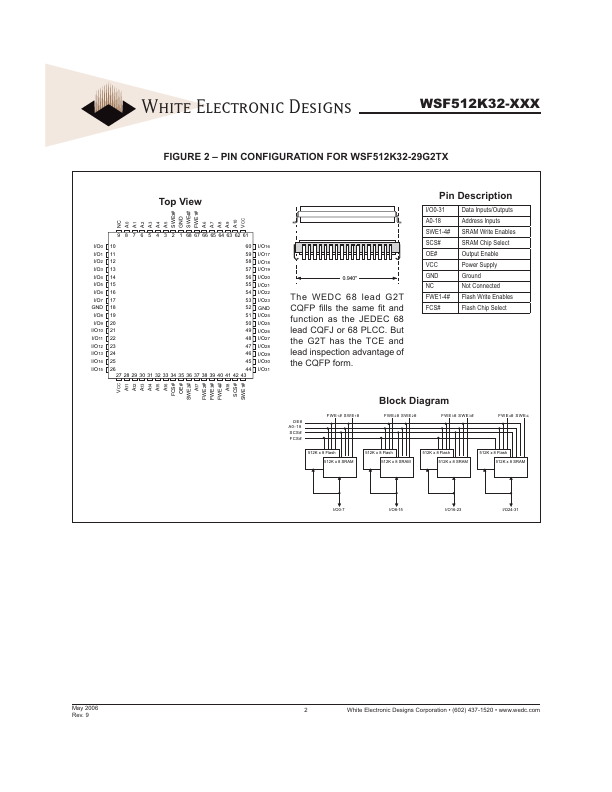
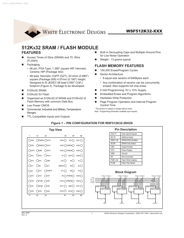
Access Times of 25ns (SRAM) and 70, 90ns (FLASH) Packaging • 66 pin, PGA Type, 1.385" square HIP, Hermetic Ceramic HIP (Package 402) • 68 lead, Hermetic CQFP (G2T), 22.4mm (0.880") square (Package 509) 4.57mm (0.180") height. Designed to fit JEDEC 68 lead 0.990" CQFJ footprint (Figure 2). Package to be developed.
 WSF512K32-XXX Datasheet