WCSS0232V1P
Features
- Supports 133-MHz bus for Pentium® and Power PC™ operations with zero wait states
- Fully registered inputs and outputs for pipelined operation
- 64K x 32 mon I/O architecture
- Single 3.3V power supply
- Fast clock-to-output times
..
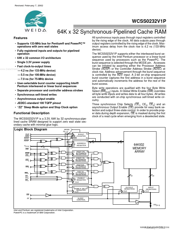
All synchronous inputs pass through input registers controlled by the rising edge of the clock. All data outputs pass through output registers controlled by the rising edge of the clock. Maximum access delay from the clock rise is 4.2 ns (133-MHz device). The WCSS0232V1P supports either the interleaved burst sequence used by the Intel Pentium processor or a linear burst sequence used by processors such as the Power PC. The burst sequence is selected through the MODE pin. Accesses can be initiated by asserting either the Processor Address Strobe (ADSP) or the Controller Address Strobe (ADSC) at clock rise. Address advancement through the burst sequence is controlled by the ADV input. A 2-bit on-chip wraparound burst counter captures the first...