S913
Features
Integrated gate protection diodes Low noise figure High gain Biasing network on chip
D Improved cross modulation at gain reduction D High AGC-range D SMD package
94 9279
13 579
94 9278
95 10831
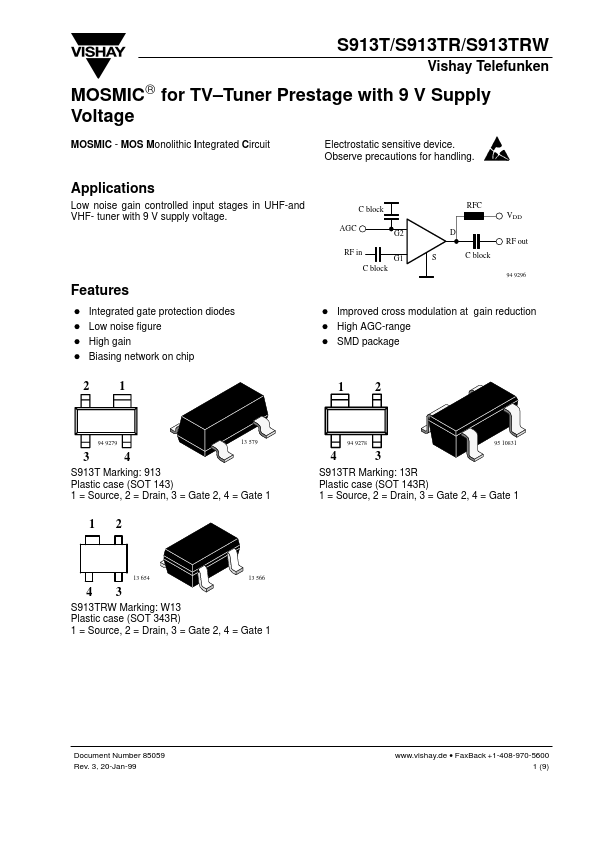
S913T Marking: 913 Plastic case (SOT 143) 1 = Source, 2 = Drain, 3 = Gate 2, 4 = Gate 1
S913TR Marking: 13R Plastic case (SOT 143R) 1 = Source, 2 = Drain, 3 = Gate 2, 4 = Gate 1
13 654
13 566
S913TRW Marking: W13 Plastic case (SOT 343R) 1 = Source, 2 = Drain, 3 = Gate 2, 4 = Gate 1
Document Number 85059 Rev. 3, 20-Jan-99
.vishay.de
- Fax Back +1-408-970-5600 1 (9)
S913T/S913TR/S913TRW
Vishay Telefunken Absolute Maximum Ratings
Tamb = 25_C, unless otherwise specified Parameter Drain
- source voltage Drain current Gate 1/Gate 2
- source peak current Gate 1/Gate 2
- source voltage Total power dissipation Channel temperature Storage temperature range Test Conditions Symbol Value VDS 12 ID 30 ±IG1/G2SM 10 ±VG1/G2SM 6 Ptot 200 TCh 150...