VBE2102M
FEATURES
- Halogen-free According to IEC 61249-2-21
Definition
- Trench Power MOSFET
- 100 % Rg and UIS Tested
- pliant to Ro HS Directive 2002/95/EC
APPLICATIONS
- Power Switch
- DC/DC Converters
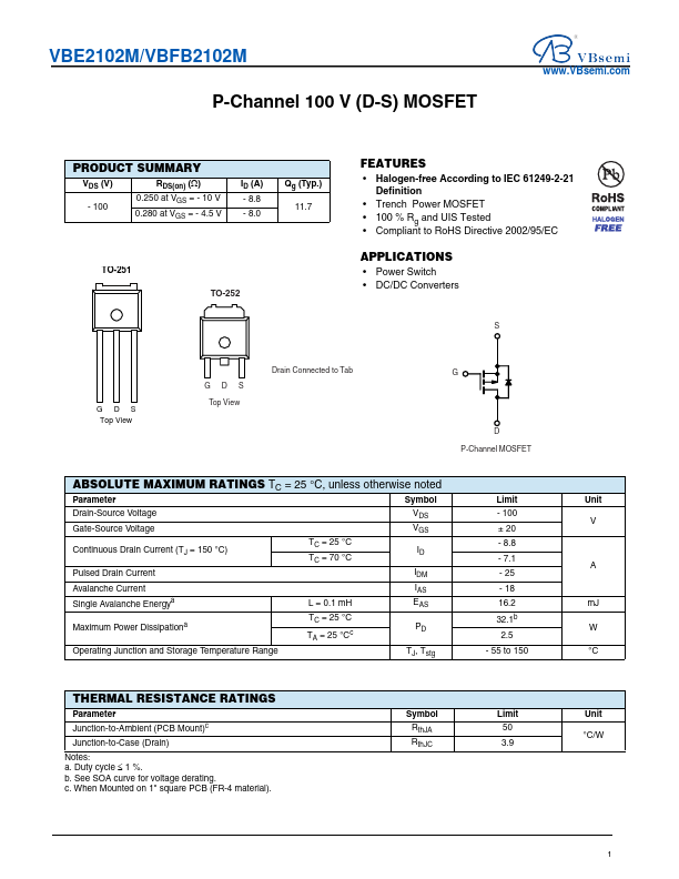
GDS Top View
GDS Top View
Drain Connected to Tab
D P-Channel MOSFET
ABSOLUTE MAXIMUM RATINGS TC = 25 °C, unless otherwise noted
Parameter
Symbol
Limit
Unit
Drain-Source Voltage Gate-Source Voltage
- 100
± 20
Continuous Drain Current (TJ = 150 °C) Pulsed Drain Current
TC = 25 °C TC = 70 °C
- 8.8
- 7.1
- 25
Avalanche Current
- 18
Single Avalanche Energya
L = 0.1 m...