Click to expand full text
VBC6N2022
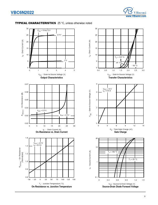
Dual N-Channel 25-V (D-S) MOSFET
www.VBsemi.com
PRODUCT SUMMARY
VDS (V)
RDS(on) (Ω)
0.022 at VGS = 4.5 V 25
0.032 at VGS = 2.5 V
ID (A) 6.6 5.5
FEATURES
• Halogen-free Option Available • TrenchFET® Power MOSFETs
Pb-free Available
RoHS*
COMPLIANT
D1 S1 2 S1 3 G1 4
TSSOP-8 Top View
8D 7 S2 6 S2 5 G2
D
D
G1
G2
S1
S2
ABSOLUTE MAXIMUM RATINGS TA = 25 °C, unless otherwise noted
Parameter
Symbol
10 s
Steady State
Unit
Drain-Source Voltage Gate-Source Voltage
VDS
25
V
VGS
± 12
Continuous Drain Current (TJ = 150 °C)a Pulsed Drain Current
TA = 25 °C TA = 70 °C
ID
6.6
5.2
5.5
3.5
A
IDM
30
Continuous Source Current (Diode Conduction)a
IS
1.5
1.0
Maximum Power Dissipationa
TA = 25 °C TA = 70 °C
PD
1.5
1.0
0.96
0.
 VBC6N2022 Datasheet