Click to expand full text
9567GH-VB
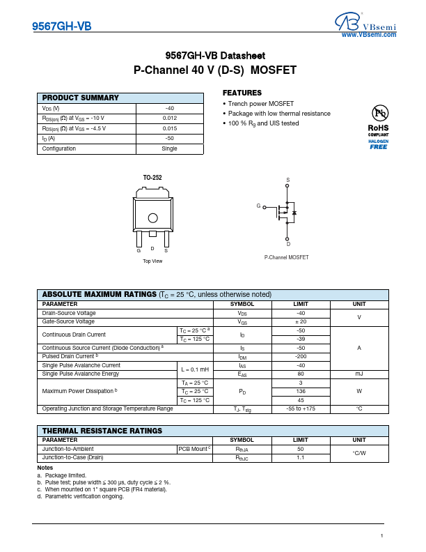
9567GH-VB Datasheet
P-Channel 4 0 V (D-S) MOSFET
www.VBsemi.com
PRODUCT SUMMARY
VDS (V) RDS(on) () at VGS = -10 V RDS(on) () at VGS = -4.5 V ID (A) Configuration
-40 0.012 0.015 -50 Single
FEATURES • Trench power MOSFET • Package with low thermal resistance • 100 % Rg and UIS tested
TO-252
S G
GDS Top View
D P-Channel MOSFET
ABSOLUTE MAXIMUM RATINGS (TC = 25 °C, unless otherwise noted)
PARAMETER
SYMBOL
Drain-Source Voltage Gate-Source Voltage Continuous Drain Current Continuous Source Current (Diode Conduction) a Pulsed Drain Current b Single Pulse Avalanche Current Single Pulse Avalanche Energy
Maximum Power Dissipation b
Operating Junction and Storage Temperature Range
TC = 25 °C a TC = 125 °C
L = 0.
 9567GH Datasheet