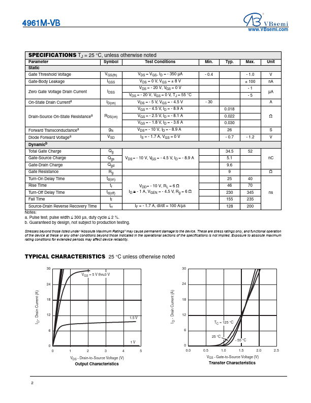
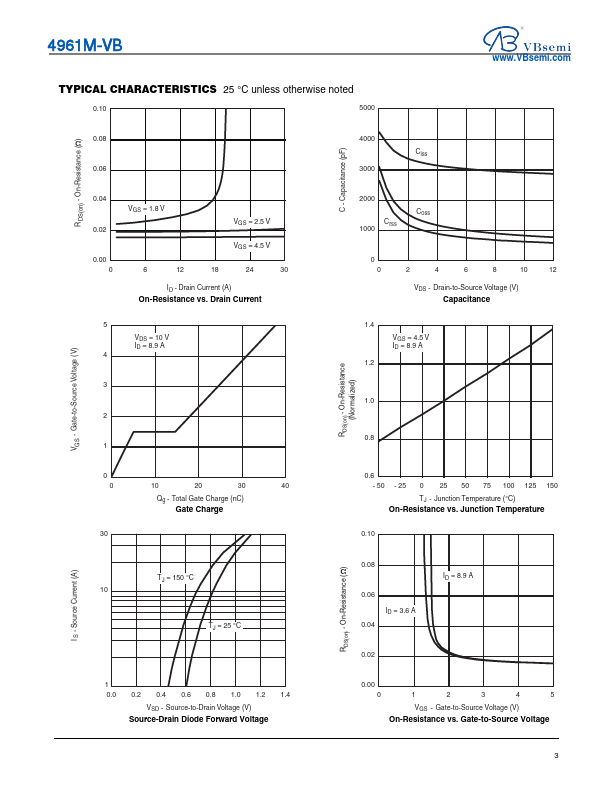
The following content is an automatically extracted verbatim text
from the original manufacturer datasheet and is provided for reference purposes only.
View original datasheet text
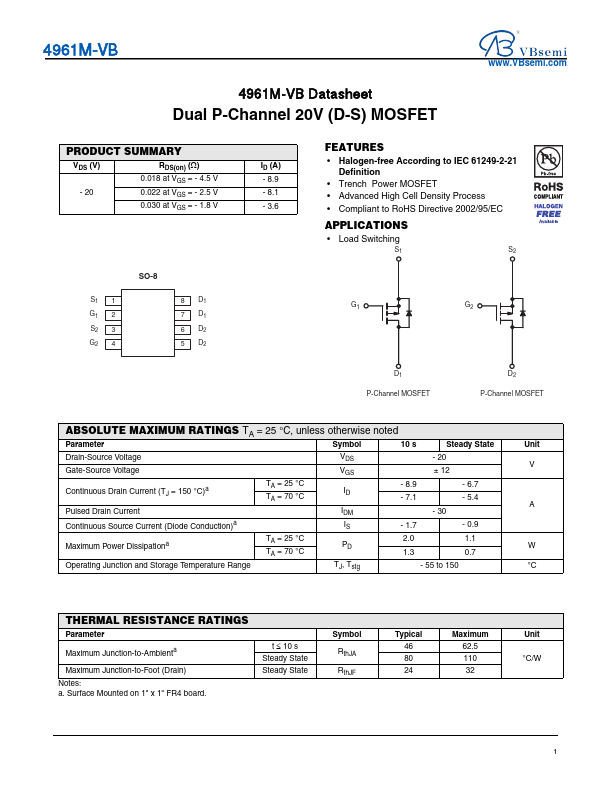
4961M-VB
4961M-VB Datasheet
Dual P-Channel 20V (D-S) MOSFET
www.VBsemi.com
PRODUCT SUMMARY
VDS (V)
RDS(on) (Ω)
0.018 at VGS = - 4.5 V
- 20
0.022 at VGS = - 2.5 V
0.030 at VGS = - 1.8 V
S1 1 G1 2 S2 3 G2 4
SO-8
8 D1 7 D1 6 D2 5 D2
ID (A) - 8.9 - 8.1 - 3.6
FEATURES
• Halogen-free According to IEC 61249-2-21 Definition
• Trench Power MOSFET • Advanced High Cell Density Process • Compliant to RoHS Directive 2002/95/EC
APPLICATIONS
• Load Switching
S1
S2
G1
G2
D1 P-Channel MOSFET
D2 P-Channel MOSFET
ABSOLUTE MAXIMUM RATINGS TA = 25 °C, unless otherwise noted
Parameter
Symbol
10 s
Steady State
Unit
Drain-Source Voltage Gate-Source Voltage
VDS
- 20
V
VGS
± 12
Continuous Drain Current (TJ = 150 °C)a Pulsed Drain Current
TA = 25 °C TA = 70 °C
ID
- 8.9 - 7.
 4961M Datasheet