Click to expand full text
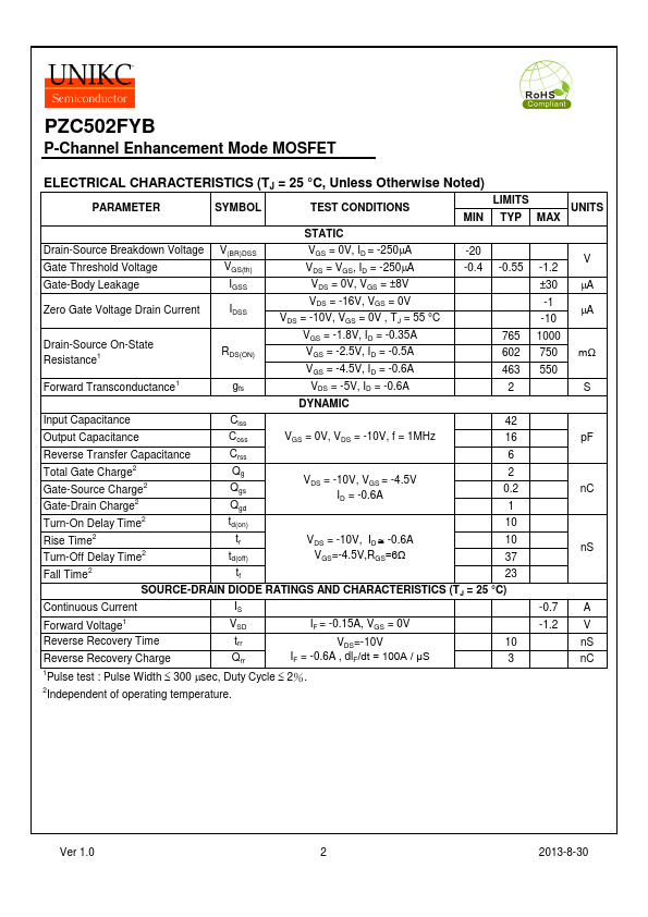
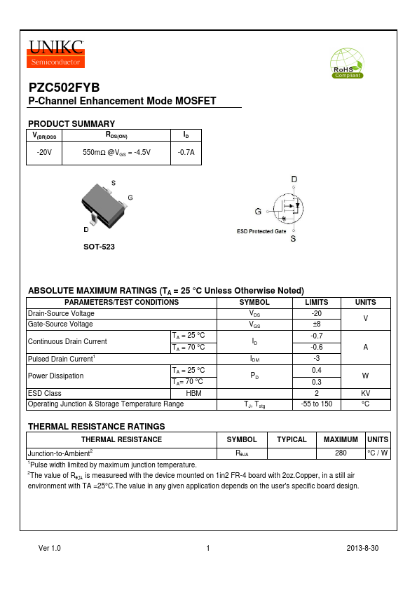
PZC502FYB
P-Channel Enhancement Mode MOSFET
PRODUCT SUMMARY
V(BR)DSS
RDS(ON)
-20V
550mΩ @VGS = -4.5V
ID -0.7A
SOT-523
ABSOLUTE MAXIMUM RATINGS (TA = 25 °C Unless Otherwise Noted)
PARAMETERS/TEST CONDITIONS
SYMBOL
LIMITS
Drain-Source Voltage
VDS -20
Gate-Source Voltage
VGS ±8
Continuous Drain Current Pulsed Drain Current1
TA = 25 °C TA = 70 °C
ID IDM
-0.7 -0.6 -3
Power Dissipation
TA = 25 °C TA= 70 °C
PD
0.4 0.3
ESD Class
HBM
2
Operating Junction & Storage Temperature Range
TJ, Tstg
-55 to 150
UNITS V
A
W KV °C
THERMAL RESISTANCE RATINGS
THERMAL RESISTANCE
SYMBOL
TYPICAL MAXIMUM UNITS
Junction-to-Ambient2
RqJA
280
1Pulse width limited by maximum junction temperature.
2The value of RqJA is measureed with the device mounted on 1in2 FR-4 board with 2oz.
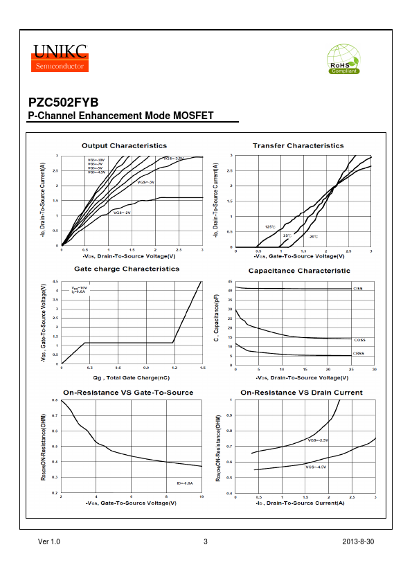
 PZC502FYB Datasheet