Full PDF Text Transcription for P2402OV (Reference)
Note: Below is a high-fidelity text extraction (approx. 800 characters) for
P2402OV. For precise diagrams, and layout, please refer to the original PDF.
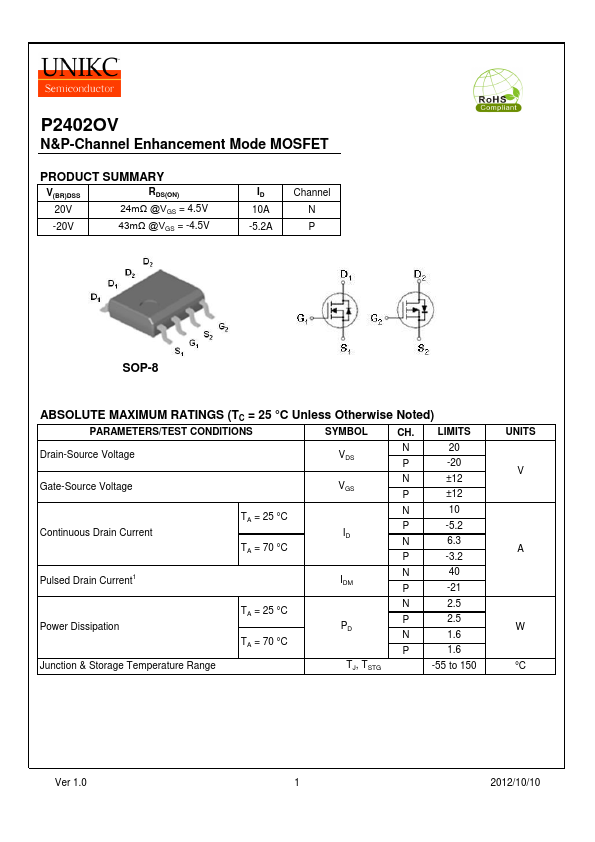
P2402OV N&P-Channel Enhancement Mode MOSFET PRODUCT SUMMARY V(BR)DSS 20V RDS(ON) 24mΩ @VGS = 4.5V -20V 43mΩ @VGS = -4.5V ID 10A -5.2A Channel N P SOP-8 ABSOLUTE MAXIMUM R...
View more extracted text
0V 43mΩ @VGS = -4.5V ID 10A -5.2A Channel N P SOP-8 ABSOLUTE MAXIMUM RATINGS (TC = 25 °C Unless Otherwise Noted) PARAMETERS/TEST CONDITIONS SYMBOL CH. LIMITS Drain-Source Voltage N 20 VDS P -20 Gate-Source Voltage N ±12 VGS P ±12 Continuous Drain Current TA = 25 °C TA = 70 °C N 10 P -5.2 ID N 6.3 P -3.2 Pulsed Drain Current1 N 40 IDM P -21 Power Dissipation TA = 25 °C TA = 70 °C N 2.5 P 2.5 PD N 1.6 P 1.6 Junction & Storage Temperature Range TJ, TSTG -55 to 150 UNITS V A W °C Ver 1.0 1 2012/10/10 P2402OV N&P-Channel Enhancement Mode MOSFET THERMAL RESISTANCE RATINGS THERMAL RESISTANCE Junction-to-Ambient 1Pulse width limit
 P2402OV Datasheet