IRFR8314TR
Features
VDS(V)=30V ID=90A(VGS=10V) RDS(ON)<2.2mΩ(VGS=10V) RDS(ON)<3.1mΩ(VGS=4.5V)
2.Application
Optimized for UPS/Inverter Applications
Lead-Free, Ro HS pliant Fully Characterized Avalanche Voltage and Current
Low Voltage Power Tools
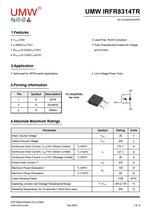
3.Pinning information
Pin
Symbol Description
TO-252(DPAK) top view
GATE
SOURCE
DRAIN
4.Absolute Maximum Ratings
Parameter
Drain- Source Voltage
Gate-to-Source Voltage
Continuous Drain Current, VGS=10V (Silicon Limited)
TC=25°C
Continuous Drain Current, VGS=10V (Silicon Limited) Continuous Drain Current, VGS=10V (Package Limited) Pulsed Drain Current ç
TC=100°C TC=25°C
Maximum Power Dissipation Maximum Power Dissipation Linear Derating Factor
TC=25°C TC=100°C
Operating Junction and Storage Temperature Range
Soldering Temperature, for 10 seconds (1.6mm from case)
Symbol VDS VGS
IDM PD
TJ, TSTG
Rating 30 ±20
179 æ 127 æ
90 357 125 63 0.83 -55 to 175 300
Units V V A A A A W W
W/°C °C °C
UTD Semiconductor...