FDS4435
Description
This device is well suited for Power Management and load switching applications mon in Notebook puters and Portable Battery Packs.
Features
- VDS (V) =-30V
- ID= -8.8 A(VGS = -10V)
- RDS(ON) < 20mΩ(VGS=-10V)
- RDS(ON) < 35 mΩ(VGS=-4.5V)
FDS4435 -30V P-Channel MOSFET
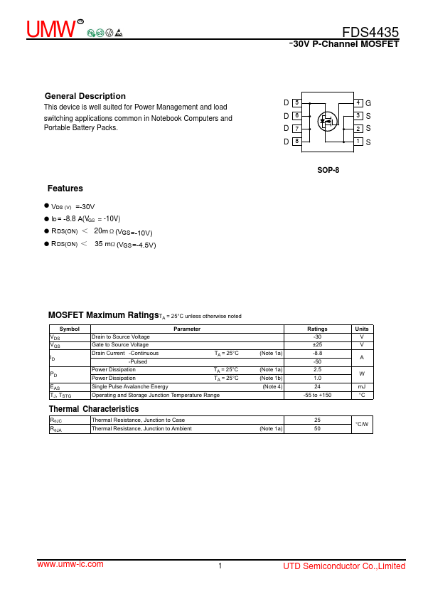
D5 D6 D7 D8
4G 3S 2S 1S
SOP-8
MOSFET Maximum Ratings TA = 25°C unless otherwise noted
Symbol VDS VGS ID
EAS TJ, TSTG
Parameter
Drain to Source Voltage
Gate to Source Voltage
Drain Current -Continuous -Pulsed
TA = 25°C
Power Dissipation Power Dissipation Single Pulse Avalanche Energy
TA = 25°C TA = 25°C
Operating and Storage Junction Temperature Range
Thermal Characteristics
RTJC RTJA
Thermal Resistance, Junction to Case Thermal Resistance, Junction to Ambient
(Note 1a) (Note 1a) (Note 1b)
(Note 4)
(Note 1a)
Ratings -30 ±25 -8.8 -50 2.5 1.0 24
-55 to +150
25 50
Units V V A
W m J °C
°C/W
.umw-ic.
UTD Semiconductor Co.,Limited
UMW R
FDS4435 -30V P-Channel...