FDS3672
Features
ID=7.5A RDS(ON)=23mΩ(VGS=10V) Qg(tot) = 28n C(Typ.),VGS=10V Low Miller Charge
2.Applications
DC/DC converters and Off-Line UPS Distributed Power Architectures and VRMs
Low Qrr Body Diode Optimized efficiency at high frequencies UIS Capability (Single Pulse and Repetitive Pulse)
Primary Switch for 24V and 48V Systems High Voltage Synchronous Rectifier
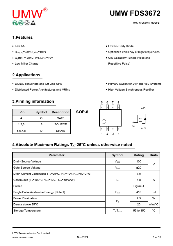
3.Pinning information
Pin 4 1,2,3 5,6,7,8
Symbol G S D
Description
GATE
SOURCE DRAIN
SOP-8
4.Absolute Maximum Ratings TA=25°C unless otherwise noted
Parameter Drain-Source Voltage Gate-Source Voltage Drain Current Continuous (TA=25°C, VGS=10V, RθJA=50°C/W) Continuous (TA=100°C, VGS=10V, RθJA=50°C/W) Pulsed Single Pulse Avalanche Energy (Note 1) Power Dissipation Derate above 25°C Storage Temperature
Symbol VDSS VGS
EAS PD TJ,TSTG
Rating Units
100 V
±20
Figure 4
416 m J
20 m W/°C
-55 to 150 °C
UTD Semiconductor Co.,Limited .umw-ic.
Nov.2024
1 of...