High Density Cell Design for Ultra Low On-Resistance.
Lead free product is acquired.
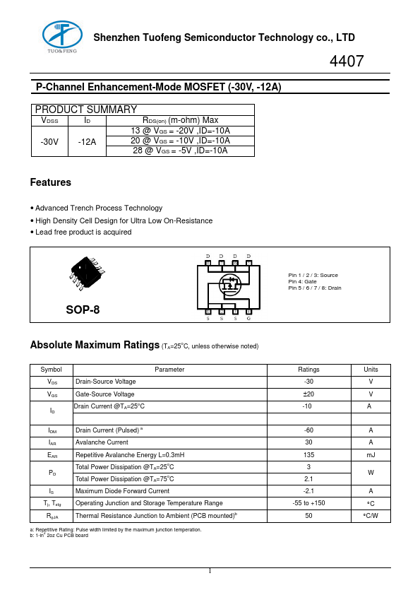
SOP-8
Absolute Maximum Ratings (TA=25oC, unless otherwise noted)
Symbol VDS VGS
ID
Drain-Source Voltage Gate-Source Voltage Drain Current @TA=25oC
Parameter
IDM Drain Current (Pulsed) a IAR Avalanche Current EAR Repetitive Avalanche Energy L=0.3mH
Total Power Dissipation @TA=25oC PD Total Power Dissipation @TA=75oC IS Maximum Diode Forward Current.
A) PRODUCT SUMMARY VDSS ID RDS(on) (m-ohm) Max 13 @ VGS = -20V ,ID=-10A -30V -12A 20 @ VGS = -10V ,ID=-10A 28 @ VGS = -5V ,ID=-10A Features · Advanced Trench Process Technology · High Density Cell Design for Ultra Low On-Resistance · Lead free product is acquired · SOP-8 Absolute Maximum Ratings (TA=25oC, unless otherwise noted) Symbol VDS VGS ID Drain-Source Voltage Gate-Source Voltage Drain Current @TA=25oC Parameter IDM Drain Current (Pulsed) a IAR Avalanche Current EAR Repetitive Avalanche Energy L=0.
 4407 Datasheet