Datasheet Details
| Part number | TQP9113 |
|---|---|
| Manufacturer | TriQuint Semiconductor |
| File Size | 635.54 KB |
| Description | 1 Watt Linear Amplifier |
| Datasheet |
 TQP9113 Datasheet TQP9113 Datasheet
|
|
|
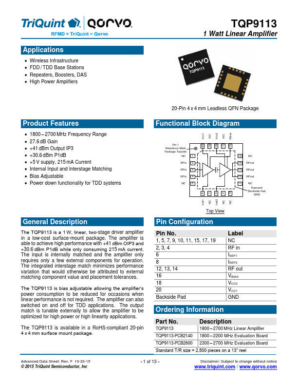
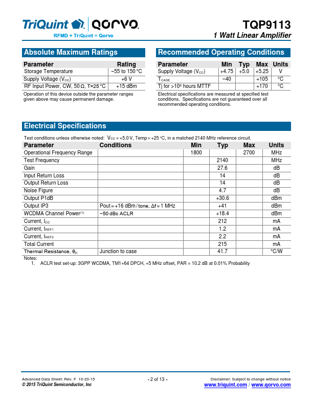
The TQP9113 is a 1 W, linear, two-stage driver amplifier in a low-cost surface-mount package.
The amplifier is able to achieve high performance with +41 dBm OIP3 and +30.6 dBm P1dB while only consuming 215 mA current.
| Part number | TQP9113 |
|---|---|
| Manufacturer | TriQuint Semiconductor |
| File Size | 635.54 KB |
| Description | 1 Watt Linear Amplifier |
| Datasheet |
TQP9113 Datasheet
|
|
|
|
Note: Below is a high-fidelity text extraction (approx. 800 characters) for TQP9113. For precise diagrams, and layout, please refer to the original PDF.
Applications Wireless Infrastructure FDD / TDD Base Stations Repeaters, Boosters, DAS High Power Amplifiers TQP9113 1 Watt Linear Amplifier Product Features 180...
| Part Number | Description |
|---|---|
| TQP9111 | 2 Watt Power Amplifier |
| TQP9107 | 2-stage Power Amplifier |
| TQP9108 | 2-stage Power Amplifier |
| TQP9051 | MIPI ET/APT MMPA |
| TQP9058H | Multi-Mode / Multi-Band Power Amplifier Module |
| TQP9059 | Advanced ET/APT-MIPI MMPA |
| TQP9059S | Advanced ET/APT-MIPI MMPA |
| TQP9221 | High Linearity 0.25 W Small Cell PA |
| TQP9309 | High Efficiency 0.5W Small Cell Power Amplifier |
| TQP9321 | High Efficiency 0.5 W Small Cell PA |