TW015N65C
Features
(1) Chip design of 3rd generation (Built-in Si C schottky barrier diode) (2) Low diode forward voltage: VDSF = -1.35 V (typ.) (3) High voltage: VDSS = 650 V (4) Low drain-source on-resistance: RDS(ON) = 15 mΩ (typ.) (5) Less susceptible to malfunction due to high threshold voltage: Vth = 3.0 to 5.0 V (VDS = 10 V, ID = 11.7 m A) (6) Remended gate
- source drive voltage: VGS_on = 18 V, VGS_off = 0 V (7) Enhancement mode.
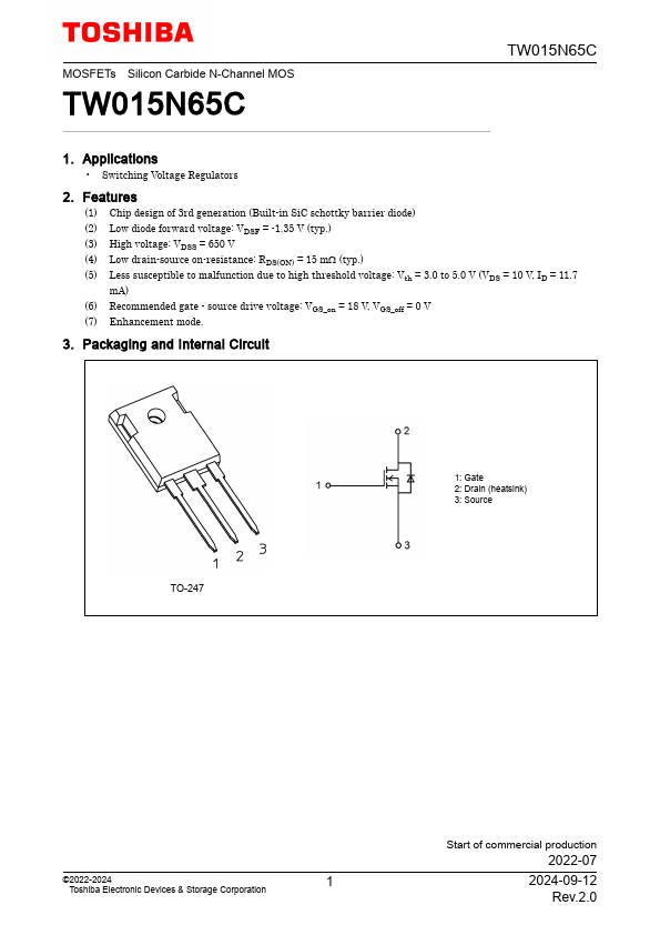
3. Packaging and Internal Circuit
TO-247
1: Gate 2: Drain (heatsink) 3: Source
©2022-2024
Toshiba Electronic Devices & Storage Corporation
Start of mercial production
2022-07
2024-09-12 Rev.2.0
4. Absolute Maximum Ratings (Note) (Ta = 25
- unless otherwise specified)
Characteristics
Symbol
Rating
Unit
Drain-source voltage Gate-source voltage Drain current (DC) Drain current (DC) Drain current (pulsed) Drain current (pulsed) Power dissipation Channel temperature Storage temperature Mounting torque
( Tc = 25
- ) ( Tc = 100- ) ( Tc = 25
- )...