Full PDF Text Transcription for TC74VHC21FN (Reference)
Note: Below is a high-fidelity text extraction (approx. 800 characters) for
TC74VHC21FN. For precise diagrams, and layout, please refer to the original PDF.
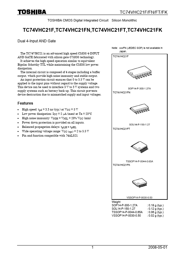
TC74VHC21F/FN/FT/FK TOSHIBA CMOS Digital Integrated Circuit Silicon Monolithic TC74VHC21F,TC74VHC21FN,TC74VHC21FT,TC74VHC21FK Dual 4-Input AND Gate The TC74VHC21 is an ad...
View more extracted text
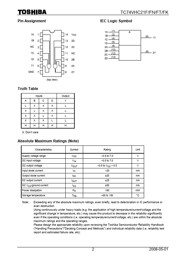
N,TC74VHC21FT,TC74VHC21FK Dual 4-Input AND Gate The TC74VHC21 is an advanced high speed CMOS 4-INPUT AND GATE fabricated with silicon gate C2MOS technology. It achieves the high speed operation similar to equivalent Bipolar Schottky TTL while maintaining the CMOS low power dissipation. The internal circuit is composed of 4 stages including a buffer output, which provide high noise immunity and stable output. An input protection circuit ensures that 0 to 5.5 V can be applied to the input pins without regard to the supply voltage. This device can be used to interface 5 V to 3 V systems and two supply systems such as battery
 TC74VHC21FN Datasheet