Click to expand full text
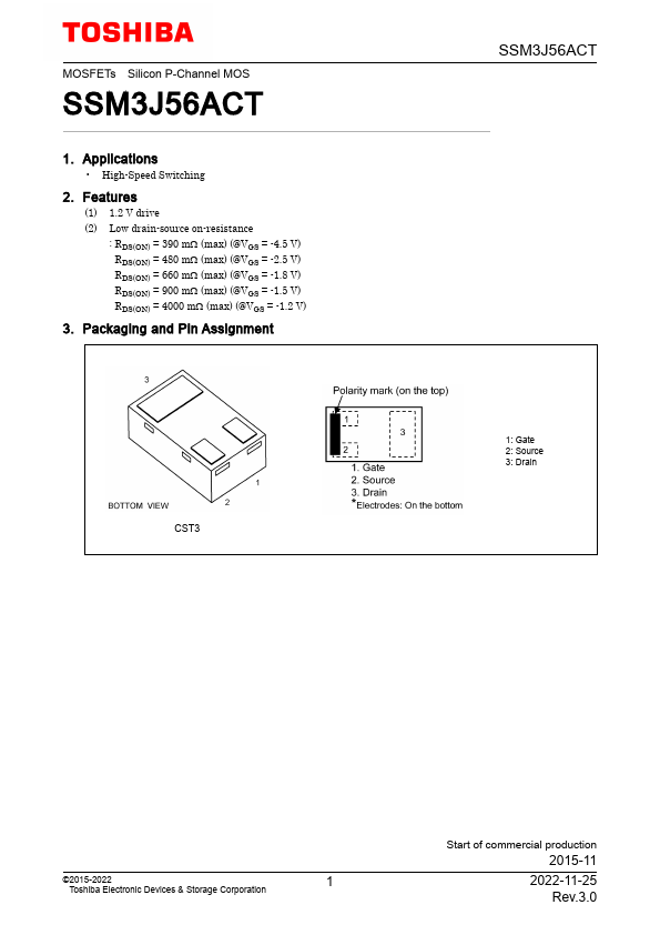
MOSFETs Silicon P-Channel MOS
SSM3J56ACT
1. Applications
• High-Speed Switching
2. Features
(1) 1.2 V drive (2) Low drain-source on-resistance
: RDS(ON) = 390 mΩ (max) (@VGS = -4.5 V) RDS(ON) = 480 mΩ (max) (@VGS = -2.5 V) RDS(ON) = 660 mΩ (max) (@VGS = -1.8 V) RDS(ON) = 900 mΩ (max) (@VGS = -1.5 V) RDS(ON) = 4000 mΩ (max) (@VGS = -1.2 V)
3. Packaging and Pin Assignment
CST3
SSM3J56ACT
1: Gate 2: Source 3: Drain
©2015-2022
1
Toshiba Electronic Devices & Storage Corporation
Start of commercial production
2015-11
2022-11-25 Rev.3.0
SSM3J56ACT
4. Absolute Maximum Ratings (Note) (Unless otherwise specified, Ta = 25 �)
Characteristics
Symbol
Rating
Unit
Drain-source voltage Gate-source voltage
VDSS
-20
V
VGSS
±8
Drain current (DC)
(Note 1)
ID
-1.
 SSM3J56ACT Datasheet