Datasheet Details
| Part number | TC74LCX07FK |
|---|---|
| Manufacturer | Toshiba |
| File Size | 280.41 KB |
| Description | Low-Voltage HEX Buffer |
| Datasheet |
 TC74LCX07FK Datasheet TC74LCX07FK Datasheet
|
|
|
Download the TC74LCX07FK datasheet PDF. This datasheet also covers the TC74LCX07F variant, as both devices belong to the same low-voltage hex buffer family and are provided as variant models within a single manufacturer datasheet.
| Part number | TC74LCX07FK |
|---|---|
| Manufacturer | Toshiba |
| File Size | 280.41 KB |
| Description | Low-Voltage HEX Buffer |
| Datasheet |
TC74LCX07FK Datasheet
|
|
|
|
Note: Below is a high-fidelity text extraction (approx. 800 characters) for TC74LCX07FK. For precise diagrams, and layout, please refer to the original PDF.
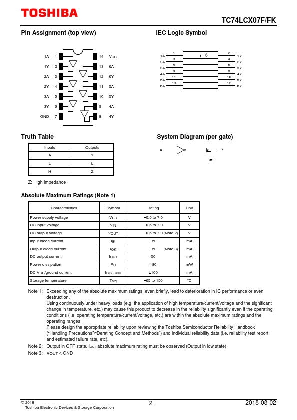
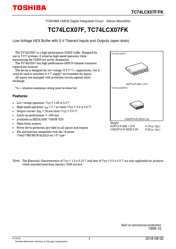
TC74LCX07F/FK TOSHIBA CMOS Digital Integrated Circuit Silicon Monolithic TC74LCX07F, TC74LCX07FK Low-Voltage HEX Buffer with 5-V Tolerant Inputs and Outputs (open drain) ...
| Part Number | Description |
|---|---|
| TC74LCX07F | Low-Voltage HEX Buffer |
| TC74LCX00F | Low-Voltage Quad 2-Input NAND Gate |
| TC74LCX00FK | Low-Voltage Quad 2-Input NAND Gate |
| TC74LCX02F | Low-Voltage Quad 2-Input NOR Gate |
| TC74LCX02FK | Low-Voltage Quad 2-Input NOR Gate |
| TC74LCX04F | Low-Voltage Hex Inverter |
| TC74LCX04FK | Low-Voltage Hex Inverter |
| TC74LCX05F | Low-Voltage HEX Inverter |
| TC74LCX05FK | Low-Voltage HEX Inverter |
| TC74LCX08F | Low-Voltage Quad 2-Input AND Gate |