The following content is an automatically extracted verbatim text
from the original manufacturer datasheet and is provided for reference purposes only.
View original datasheet text
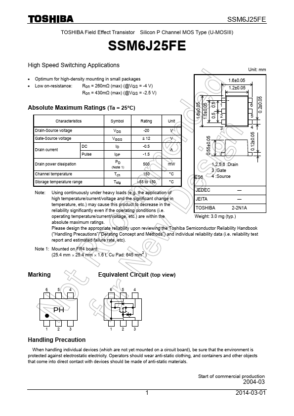
SSM6J25FE
TOSHIBA Field Effect Transistor Silicon P Channel MOS Type (U-MOSIII)
SSM6J25FE
High Speed Switching Applications
• Optimum for high-density mounting in small packages • Low on-resistance: Ron = 260mΩ (max) (@VGS = -4 V)
Ron = 430mΩ (max) (@VGS = -2.5 V)
Unit: mm
1.6±0.05 1.2±0.05
0.2±0.05
1.6±0.05 1.0±0.05 0.5 0.5
Absolute Maximum Ratings (Ta = 25°C)
1
6
Characteristics Drain-Source voltage
Symbol VDS
Rating
Unit
-20
V
2
5
3
4
0.12±0.05
0.55±0.05
Gate-Source voltage
VGSS
± 12
V
Drain current
DC
ID
-0.5
A
Pulse
IDP
-1.5
Drain power dissipation Channel temperature Storage temperature range
PD
500
mW
(Note 1)
Tch
150
°C
Tstg
−55 to 150
°C
1,2,5,6 :Drain 3 :Gate ES6 4 :Source
Note:
Using continuously under heavy loads (e.g.
 SSM6J25FE Datasheet