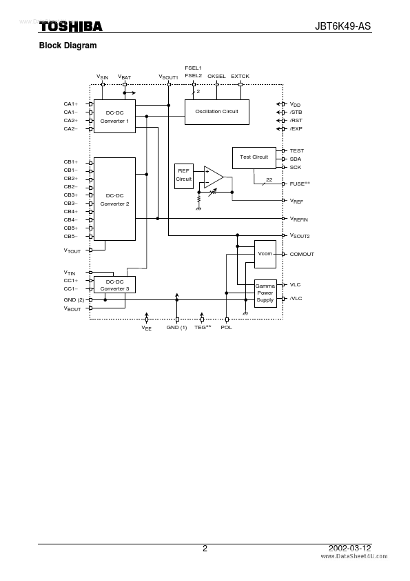
Built-in circuits : DC-DC converters and oscillation circuit for DC-DC converters High-precision regulator Binary buffer for γ-correction Level shifter circuit for Vcom.
Supply voltage (VDD) : 2.7 V to 3.3 V Supply voltage (VBAT) : 2.7 V to 4.2 V Low power consumption Operating temperature :.
20°C to 75°C CMOS process Recommended drivers : T6K47 source driver for TFT LCD T6K48 gate driver for TFT LCD Package :
Product Name JBT6K49-AS (PI) De.
The following content is an automatically extracted verbatim text
from the original manufacturer datasheet and is provided for reference purposes only.
View original datasheet text
www.DataSheet4U.com
JBT6K49-AS
TOSHIBA CMOS Digital Integrated Circuit Silicon Monolithic
JBT6K49-AS
Power supply IC for TFT LCD Panels
The JBT6K49-AS chip is an integrated circuit (IC) for generating the supply voltages necessary for a TFT LCD panel driver. When used in combination with the T6K47 source driver and the T6K48 gate driver for TFT LCD panels, the JBT6K49-AS enables the module set to operate with low power consumption. A high-speed CMOS process is employed to achieve low power consumption and high-speed operation for the JBT6K49-AS.
Features
· Built-in circuits : DC-DC converters and oscillation circuit for DC-DC converters High-precision regulator Binary buffer for γ-correction Level shifter circuit for Vcom · · · · · · · Supply voltage (VDD) : 2.7 V to 3.
 JBT6K49-AS Datasheet