The following content is an automatically extracted verbatim text
from the original manufacturer datasheet and is provided for reference purposes only.
View original datasheet text
MOSFETs Silicon Carbide N-Channel MOS
TW140Z120C
TW140Z120C
1. Applications
• Switching Voltage Regulators
2. Features
(1) Chip design of 3rd generation (Built-in SiC schottky barrier diode) (2) Low diode forward voltage: VDSF = -1.35 V (typ.) (3) High voltage: VDSS = 1200 V (4) Low drain-source on-resistance: RDS(ON) = 140 mΩ (typ.) (5) Less susceptible to malfunction due to high threshold voltage: Vth = 3.0 to 5.0 V (VDS = 10 V, ID = 1 mA) (6) Recommended gate - source drive voltage: VGS_on = 18 V, VGS_off = 0 V (7) Enhancement mode.
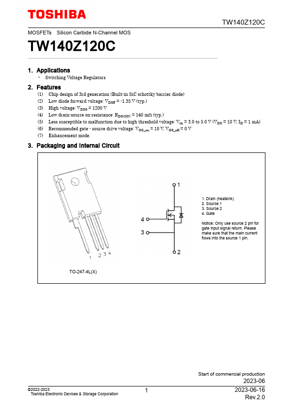
3. Packaging and Internal Circuit
TO-247-4L(X)
1. Drain (heatsink) 2. Source 1 3. Source 2 4. Gate
Notice: Only use source 2 pin for gate input signal return. Please make sure that the main current flows into the source 1 pin.
 TW140Z120C Datasheet