TW031V65C
Features
(1) Chip design of 3rd generation (Built-in Si C schottky barrier diode) (2) Low diode forward voltage: VDSF = -1.35 V (typ.) (3) High voltage: VDSS = 650 V (4) Low drain-source on-resistance: RDS(ON) = 31 mΩ (typ.) (5) Less susceptible to malfunction due to high threshold voltage: Vth = 3.0 to 5.0 V (VDS = 10 V, ID = 3 m A) (6) Remended gate
- source drive voltage: VGS_on = 18 V, VGS_off = 0 V (7) Enhancement mode.
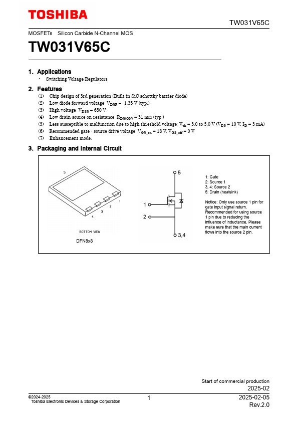
3. Packaging and Internal Circuit
DFN8x8
1: Gate 2: Source 1 3, 4: Source 2 5: Drain (heatsink)
Notice: Only use source 1 pin for gate input signal return. Remended for using source 1 pin due to reducing the influence of inductance. Please make sure that the main current flows into the source 2 pin.
©2024-2025
Toshiba Electronic Devices & Storage Corporation
Start of mercial production
2025-02
2025-02-05 Rev.2.0
4. Absolute Maximum Ratings (Note) (Ta = 25
- unless otherwise specified)
Characteristics
Symbol
Rating
Unit
Drain-source...